The AMD Vega GPU Architecture Teaser: Higher IPC, Tiling, & More, Coming in H1’2017
by Ryan Smith on January 5, 2017 9:00 AM ESTVega’s NCU: Packed Math, Higher IPC, & Higher Clocks
As always, I want to start at the heart of the matter: the shader core. In some respects AMD has not significantly altered their shader core since the launch of the very first GCN parts 5 years ago. Various iterations of GCN have added new instructions and features, but the shader core has remained largely constant, and IPC within the shader core itself hasn’t changed too much. Even Polaris (GCN 4) followed this trend, sharing its whole ISA with GCN 1.2.
With Vega, this is changing. By just how much remains to be seen, but it is clear that even with what we see today, AMD is already undertaking the biggest change to their shader core since the launch of GCN.
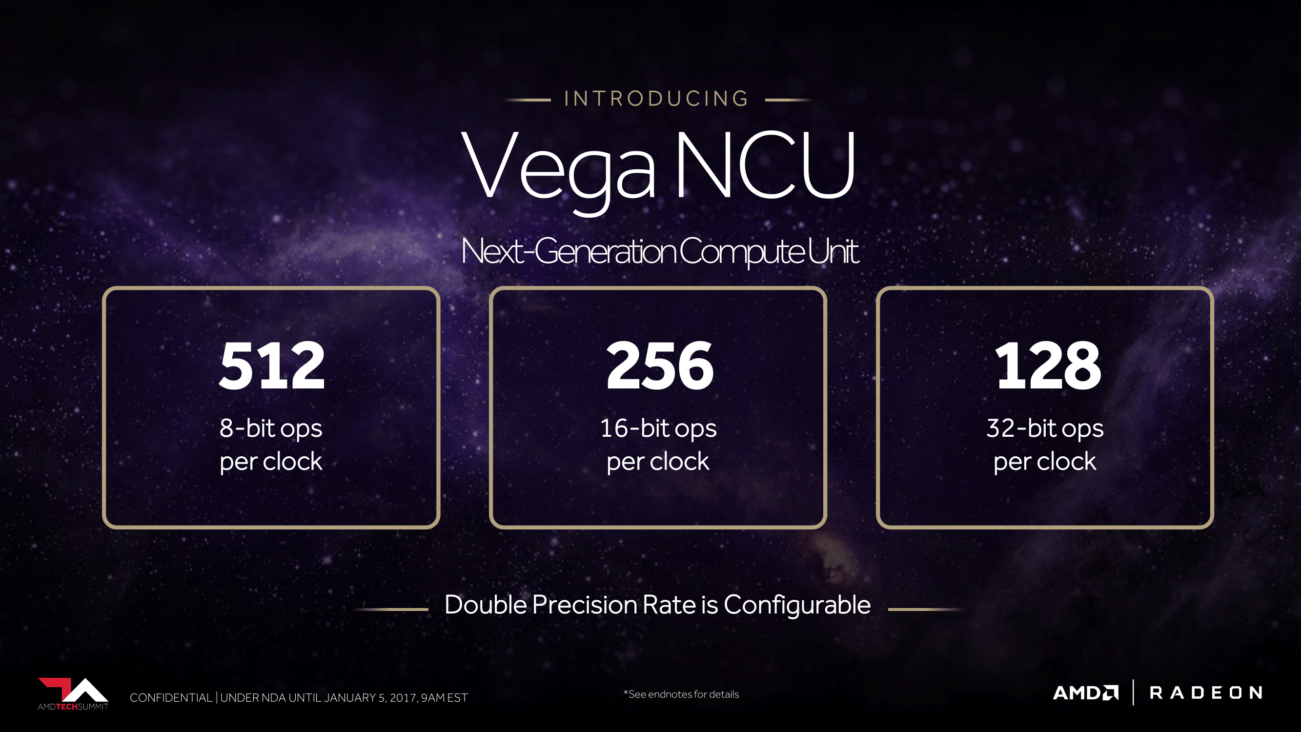
Meet the NCU, Vega’s next-generation compute unit. As we already learned from the PlayStation 4 Pro launch and last month’s Radeon Instinct announcement, AMD has been working on adding support for packed math formats for future architectures, and this is coming to fruition in Vega.
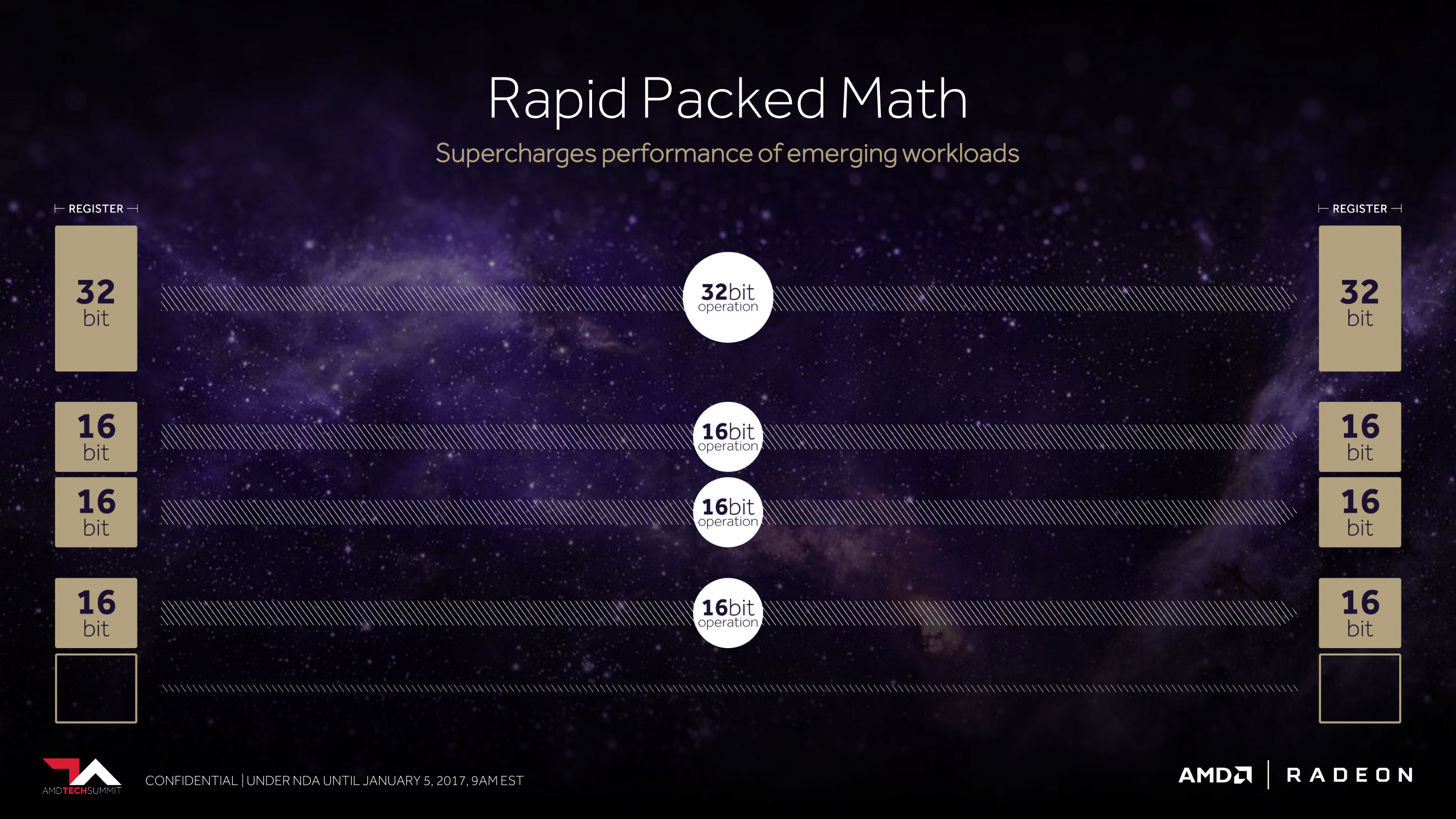
With their latest architecture, AMD is now able to handle a pair of FP16 operations inside a single FP32 ALU. This is similar to what NVIDIA has done with their high-end Pascal GP100 GPU (and Tegra X1 SoC), which allows for potentially massive improvements in FP16 throughput. If a pair of instructions are compatible – and by compatible, vendors usually mean instruction-type identical – then those instructions can be packed together on a single FP32 ALU, increasing the number of lower-precision operations that can be performed in a single clock cycle. This is an extension of AMD’s FP16 support in GCN 1.2 & GCN 4, where the company supported FP16 data types for the memory/register space savings, but FP16 operations themselves were processed no faster than FP32 operations.
And while previous announcements may have spoiled that AMD offers support for packed FP16 formats, what we haven’t known for today is that they will also support a high-speed path (analogous to packed FP16) for 8-bit integer operations. INT8 is a data format that has proven especially useful for neural network inference – the actual execution of trained neural networks – and is a major part of what has made NVIDIA’s most recent generation of Pascal GPUs so potent at inferencing. By running dot products and certain other INT8 operations along this path, INT8 performance can be greatly improved.
Though before we get too far – and this is a longer discussion to have closer to Vega’s launch – it’s always important to note when and where these faster operations can be used in consumer workloads, as the odds are most of you reading this are thinking gaming. While FP16 operations can be used for games (and in fact are in the mobile space), in the PC space they are virtually never used. When PC GPUs made the jump to unified shaders in 2006/2007, the decision was made to do everything at FP32 since that’s what vertex shaders typically required to begin with, and it’s only recently that anyone has bothered to look back. So while there is some long-term potential here for Vega’s fast FP16 math to become relevant for gaming, at the moment it wouldn’t do anything. Vega will almost certainly live and die in the gaming space based on its FP32 performance.
Moving on, the second thing we can infer from AMD’s slide is that a CU on Vega is still composed of 64 ALUs, as 128 FP32 ops/clock is the same rate as a classic GCN CU. Nothing here is said about how the Vega NCU is organized – if it’s still four 16-wide vector SIMDs – but we can at least reason out that the total size hasn’t changed.
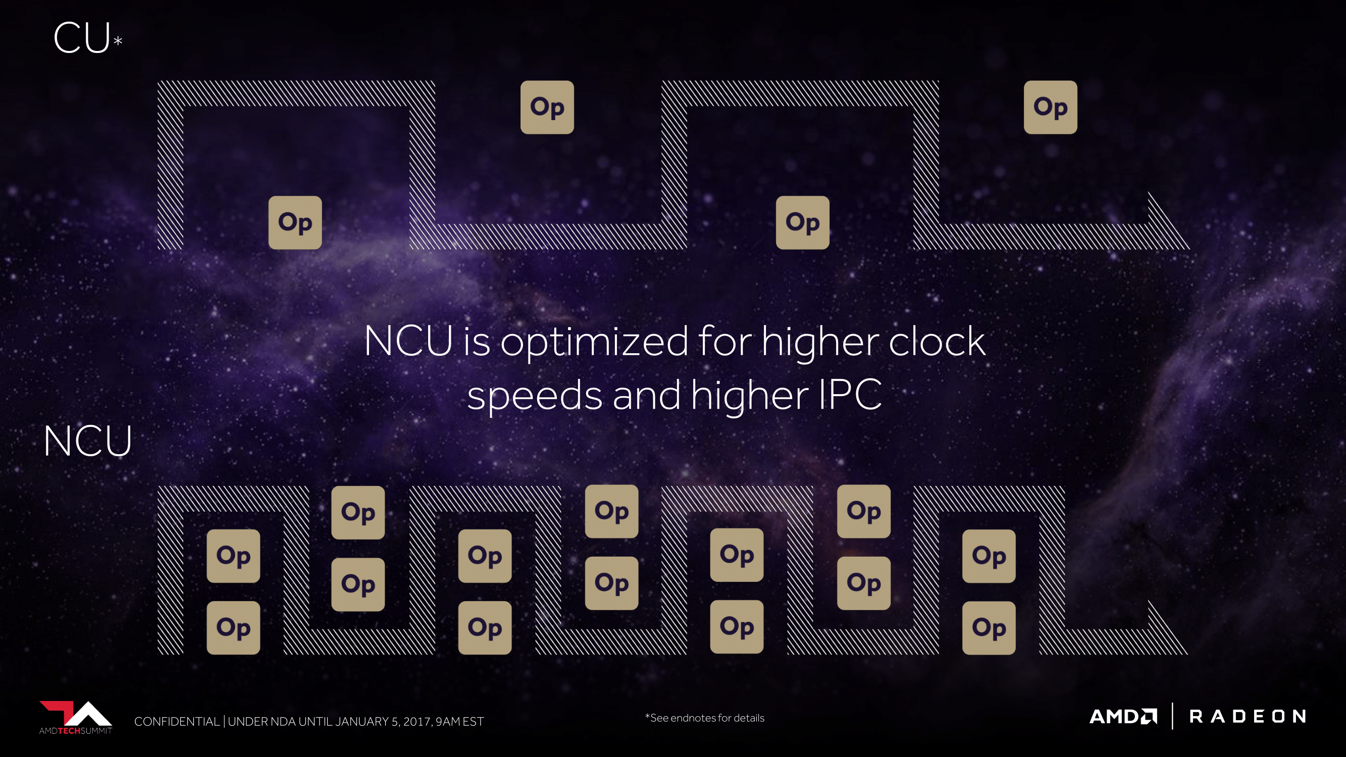
Finally, along with outlining their new packed math formats, AMD is also confirming, at a high level, that the Vega NCU is optimized for both higher clockspeeds and a higher IPC. It goes without saying that both of these are very important to overall GPU performance, and it’s an area where, very broadly speaking, AMD hasn’t compared to NVIDIA too favorably. The devil is in the details, of course, but a higher clockspeed alone would go a long way towards improving AMD’s performance. And as AMD’s IPC has been relatively stagnant for some time here, improving it would help AMD put their relatively sizable lead in total ALUs to good use. AMD has always had a good deal more ALUs than a comparable NVIDIA chip, but getting those ALUs to all do useful work outside of corner cases has always been difficult.
That said, I do think it’s important not to read too much into this on the last point, especially as AMD has drawn this slide. It’s fairly muddled whether “higher IPC” means a general increase in IPC, or if AMD is counting their packed math formats as the aforementioned IPC gain.
Geometry & Load Balancing: Faster Performance, Better Options
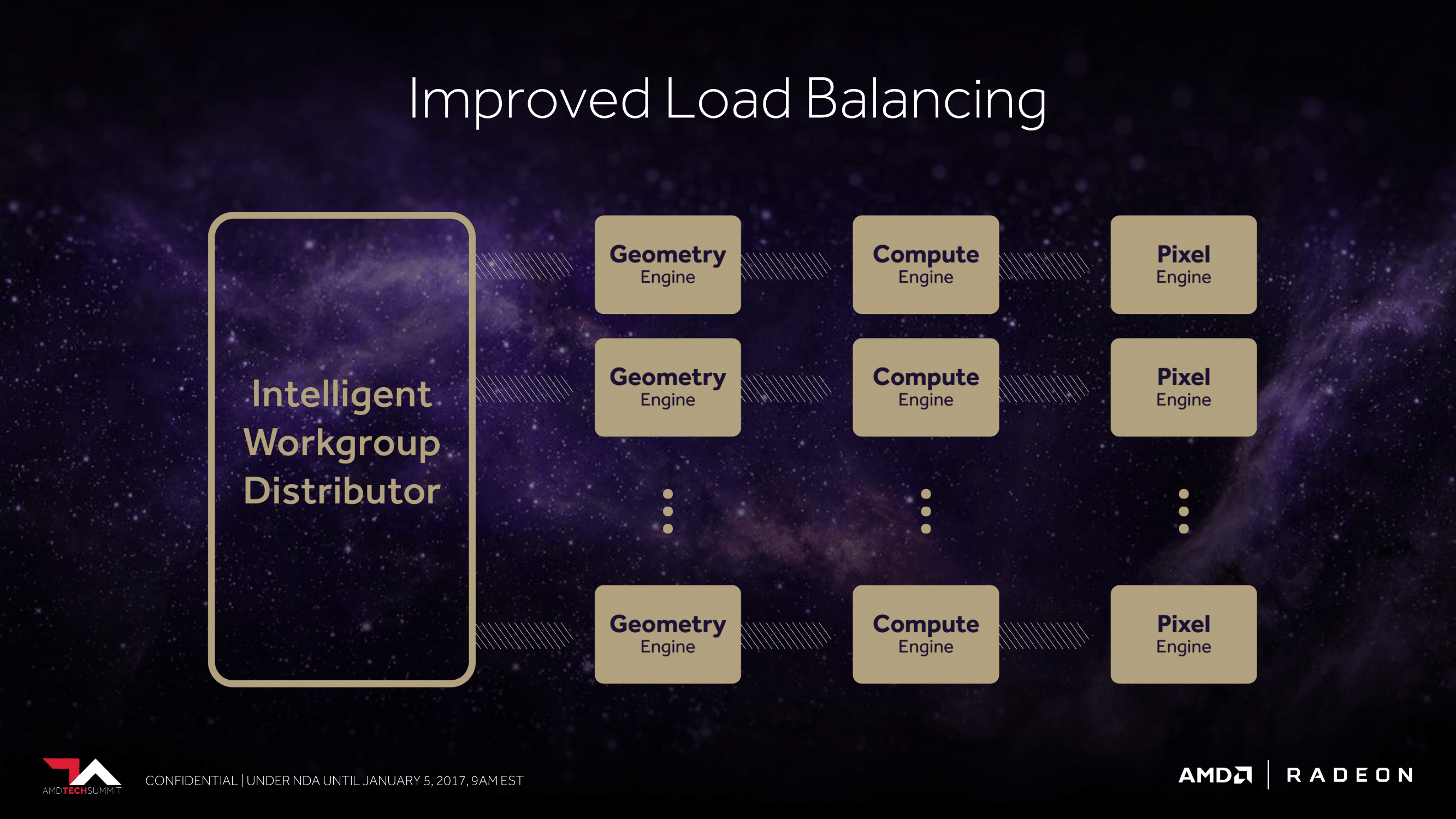
As some of our more astute readers may recall, when AMD launched the GCN 1.1 they mentioned that at the time, GCN could only scale out to 4 of what AMD called their Shader Engines; the logical workflow partitions within the GPU that bundled together a geometry engine, a rasterizer, CUs, and a set of ROPs. And when the GCN 1.2 Fiji GPU was launched, while AMD didn’t bring up this point again, they still held to a 4 shader engine design, presumably due to the fact that GCN 1.2 did not remove this limitation.
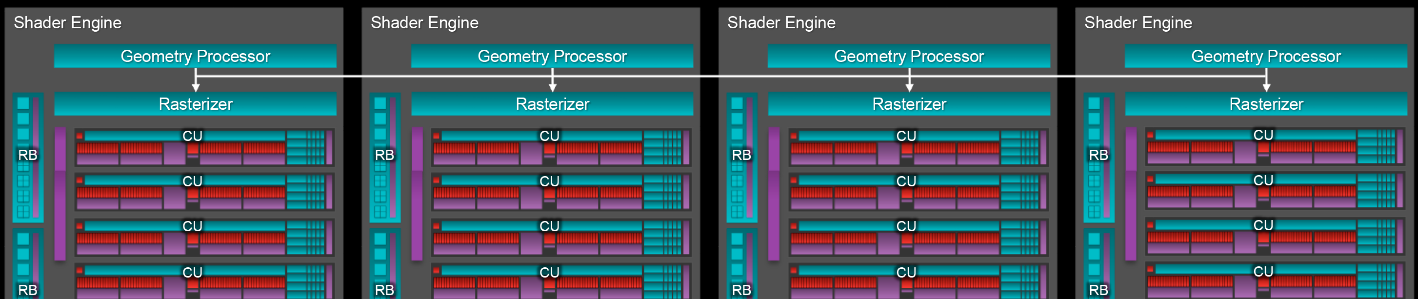
Fiji 4x Shader Engine Layout
But with Vega however, it looks like that limitation has finally gone away. AMD is teasing that Vega offers an improved load balancing mechanism, which pretty much directly hints that AMD can now efficiently distribute work over more than 4 engines. If so, this would represent a significant change in how the GCN architecture works under the hood, as work distribution is very much all about the “plumbing” of a GPU. Of the few details we do have here, AMD has told us that they are now capable of looking across draw calls and instances, to better split up work between the engines.
This in turn is a piece of the bigger picture when looking at the next improvement in Vega, which is AMD’s geometry pipeline. Overall AMD is promising a better than 2x improvement in peak geometry throughput per clock. Broadly speaking, AMD’s geometry performance in recent generations hasn’t been poor (it’s one of the areas where Polaris even further improved), but it has also hurt them at times. So this is potentially important for removing a bottleneck to squeezing more out of GCN.
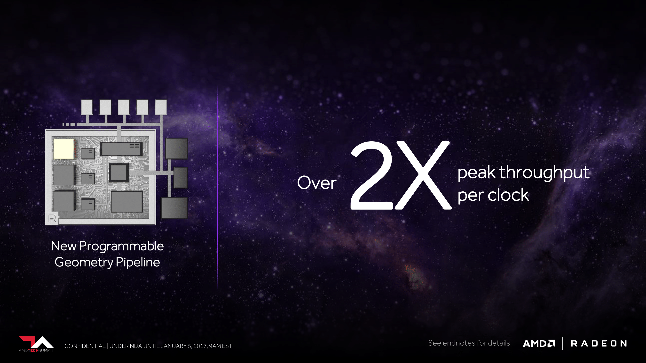
And while AMD's presentation and comments itself don't go into detail on how they achieved this increase in throughput, buried in the footnote for AMD's slide deck is this nugget: "Vega is designed to handle up to 11 polygons per clock with 4 geometry engines." So this clearly reinforces the idea that the overall geometry performance improvement in Vega comes from improving the throughput of the individual geometry engines, as opposed to simply adding more as the scalability improvements presumably allow. This is one area where Vega’s teaser paints a tantalizing view of future performance, but in the process raises further questions on just how AMD is doing it.
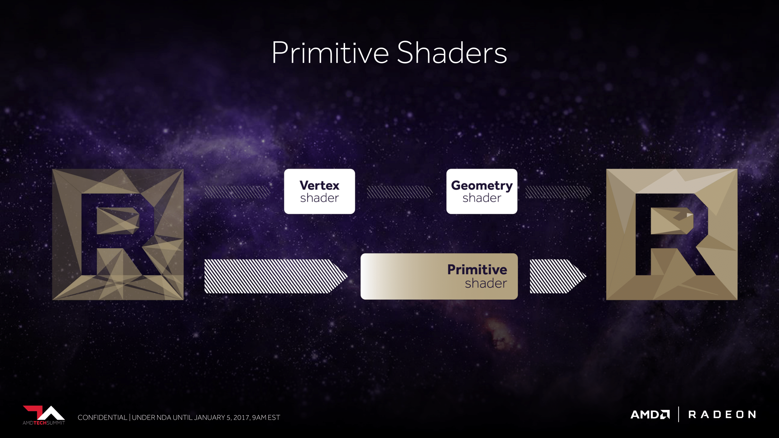
In any case, however AMD is doing it, the updated geometry engines will also feature one more advancement, which AMD is calling the primitive shader. A new shader stage that runs in place of the usual vertex and geometry shader path, the primitive shader allows for the high speed discarding of hidden/unnecessary primitives. Along with improving the total primitive rate, discarding primitives is the next best way to improve overall geometry performance, especially as game geometry gets increasingly fine, and very small, overdrawn triangles risk choking the GPU.
AMD isn’t offering any real detail here in how the primitive shader operates, and as a result I’m curious here whether this is something that AMD’s shader compiler can automatically add, or if it requires developers to specifically call it (like they would vertex and geometry shaders).


155 Comments
View All Comments
tynopik - Thursday, January 5, 2017 - link
> The first chip, which tapped out last yearI think you missed the point of my comment ;-)
should be 'taped' (one p)
wiyosaya - Thursday, January 5, 2017 - link
Mathematically speaking, the "dot product" is not defined by the number of bits in the operation. https://en.wikipedia.org/wiki/Dot_productAnonymous_87 - Thursday, January 5, 2017 - link
it is. if you consider na int8 as a 8 element vector, you can do a dot product with them.in neutral network you can assign each element of an int as in input to the network. the math involved in such network requires repetitive dot product of each element. thats what the article refers to.
bigboxes - Thursday, January 5, 2017 - link
Packed math? Well, something did get launched and something definitely got packed!Colin1497 - Thursday, January 5, 2017 - link
Last page, tapped=>taped.mr_tawan - Thursday, January 5, 2017 - link
And I just bought the Polaris (lol).Seriously I don't know how will AMD market these chips. Are they going to up against the Titan ? or the 1080/1070? or it will also replace the Rx4x0 ?
mr_tawan - Thursday, January 5, 2017 - link
AMD's GPU scheming is so psyco-crusher. (well the SF2's boss is officially Vega not M.Bison anyway).Meteor2 - Saturday, January 7, 2017 - link
They'll be RX5x0.Achaios - Thursday, January 5, 2017 - link
ARTICLE SUMMARY:- Vega to hit the shelves in June 2017.
- Speculation: 1080TI to hit the shelves around late Q3 or Q4 2017, if ever.
Buy guys, cya after 6 months.
MajGenRelativity - Thursday, January 5, 2017 - link
I'm all hyped up for Vega, but could we get a full review of the 480? I always appreciate the in-depth architectural reviews, and that would help me be prepared for Vega when it arrives.