GlobalFoundries to Expand Capacities, Build a Fab in China
by Anton Shilov on February 11, 2017 9:00 AM EST- Posted in
- Semiconductors
- GlobalFoundries
- EUV
- 7 nm
- 7nm
- FD-SOI
- FinFET
GlobalFoundries has announced plans to expand manufacturing capacities for its leading edge and mainstream production technologies in the U.S., Germany and Singapore. After the upgrades of the fabs are completed, the total 300-mm output of the company will increase by approximately 20%. In addition, GlobalFoundries intends to build a new 300mm fab in Chengdu, China, in a partnership with local authorities. The latter will produce chips using 130/180 nm and FD-SOI manufacturing technologies.
| GlobalFoundries' Expansion Plans | |||||||
| Process Technologies current and planned |
Current Capacity* wafer starts per month |
Planned Increase | Target Capacity* wafer starts per month |
Target Timeframe | |||
| Fab 1 (Dresden, Germany) |
32 nm SOI 28 nm 22FDX (FD-SOI) 12FDX (FD-SOI) |
up to 80,000 | +40% | ~110,000 | 2020 | ||
| Fab 7 (Singapore) |
130 nm 65/55 nm 40 nm RF-SOI |
68,000 | +35% for 40 nm | Over 68,000 | 2017~2018 | ||
| Fabs (Singapore) |
180 nm | unknown | +?% for 180 nm | unknown | 2017~2018 | ||
| Fab 8 (New York, USA) |
14LPP 7 nm |
up to 60,000 | +20% for 14LPP | Over 60,000 | Early 2018 | ||
| Chengdu Fab (China) |
180/130 nm 22FDX (FD-SOI) |
- | - | Ph. 1: 20,000 Ph. 2: 65,000 P1+P2: 85,000 |
Ph. 1: 2018+ Ph. 2: 2019+ |
||
| *Please note that actual wafer starts per month (WSPM) output of a fab depends on multiple factors, including process technologies used. As a result, all the WSPM capacity numbers are relative and may not reflect actual performance. Keep in mind, that as foundries and IDMs increase usage of multi-patterning techniques, their effective WSPM output drops as wafers spend more time in the cleanroom. Hence, to keep the wafer starts per month capacity, chipmakers need to add equipment (which may, or may not, involve physical expansion of the cleanroom space). | |||||||
Fab 8 to Gain 20% 14LPP FinFET Capacity
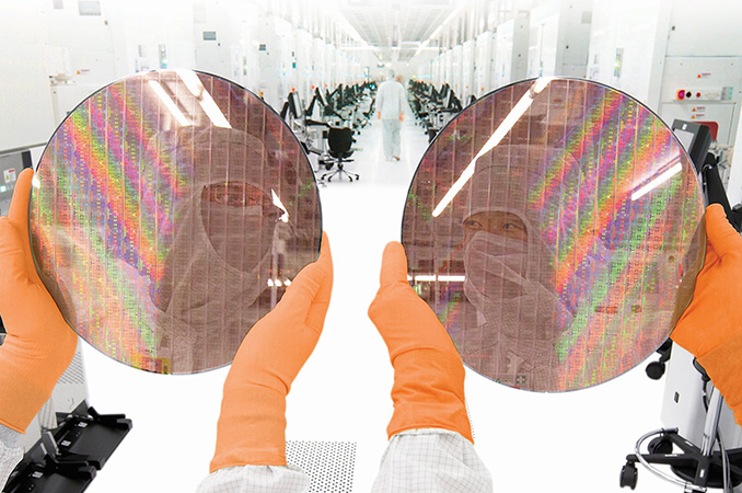
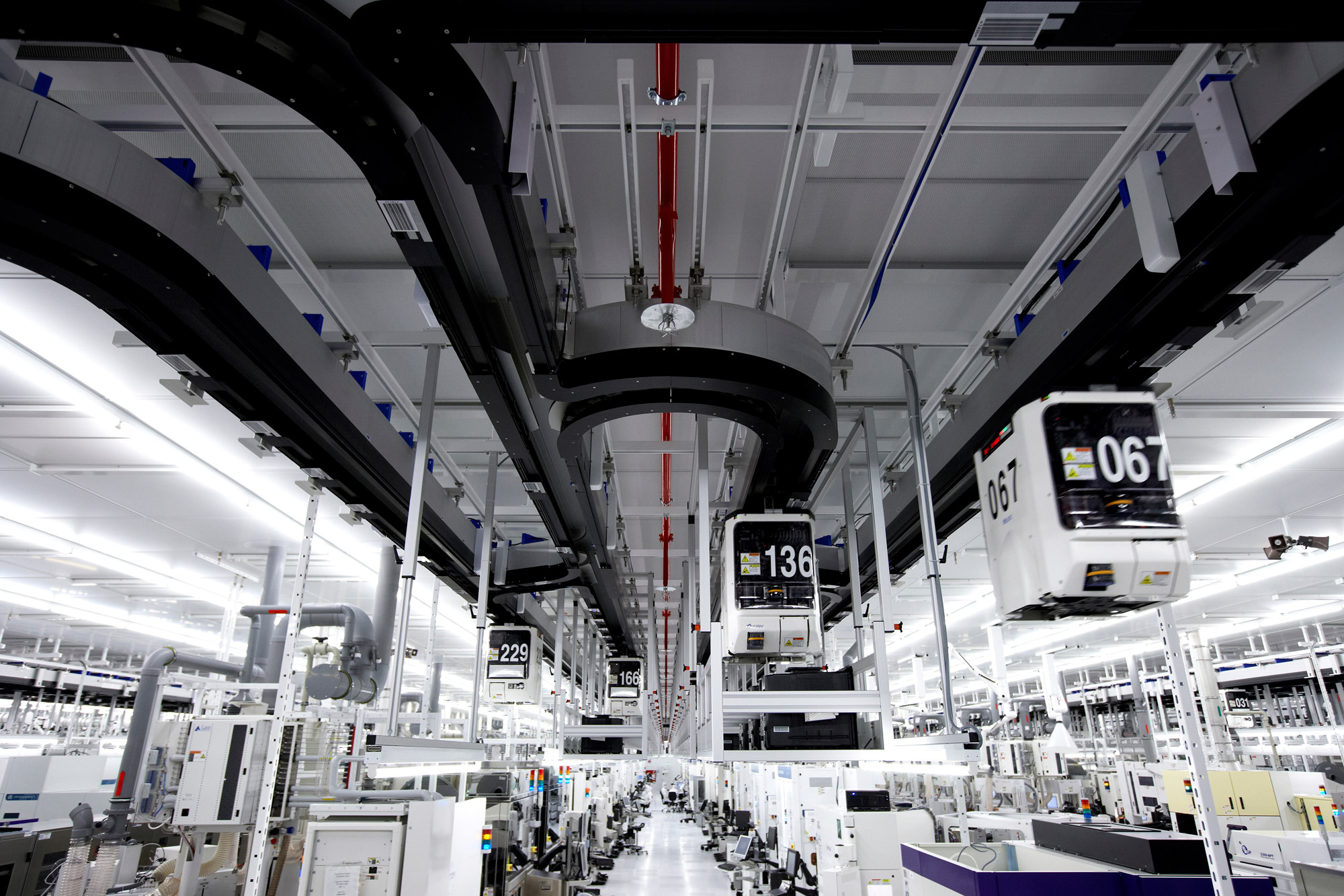
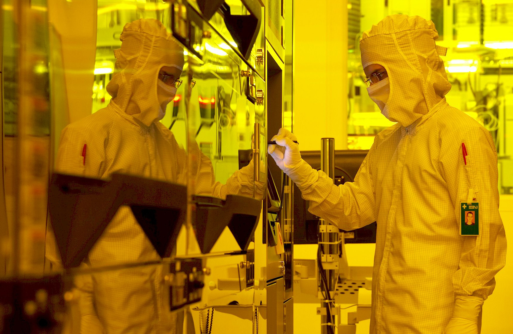
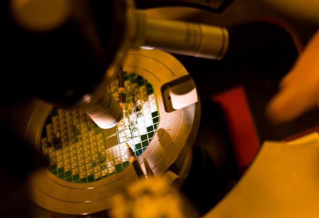
GlobalFoundries operates 10 fabs worldwide with four of them processing 300 mm wafers. The company’s most advanced fab is the Fab 8 located in Luther Forest Technology Campus (Saratoga County, New York) where the chipmaker produces flagship processors for AMD and some other leading developers of chips. To keep the Fab 8 up-to-date, GlobalFoundries spends billions of dollars on development of new manufacturing technologies and production equipment. Back in September, the company already announced plans to invest several billion in new tools to produce ICs (integrated circuits) using its 7 nm fabrication process and this week GlobalFoundries said it would invest in the expansion of the Fab 8’s manufacturing capacity.
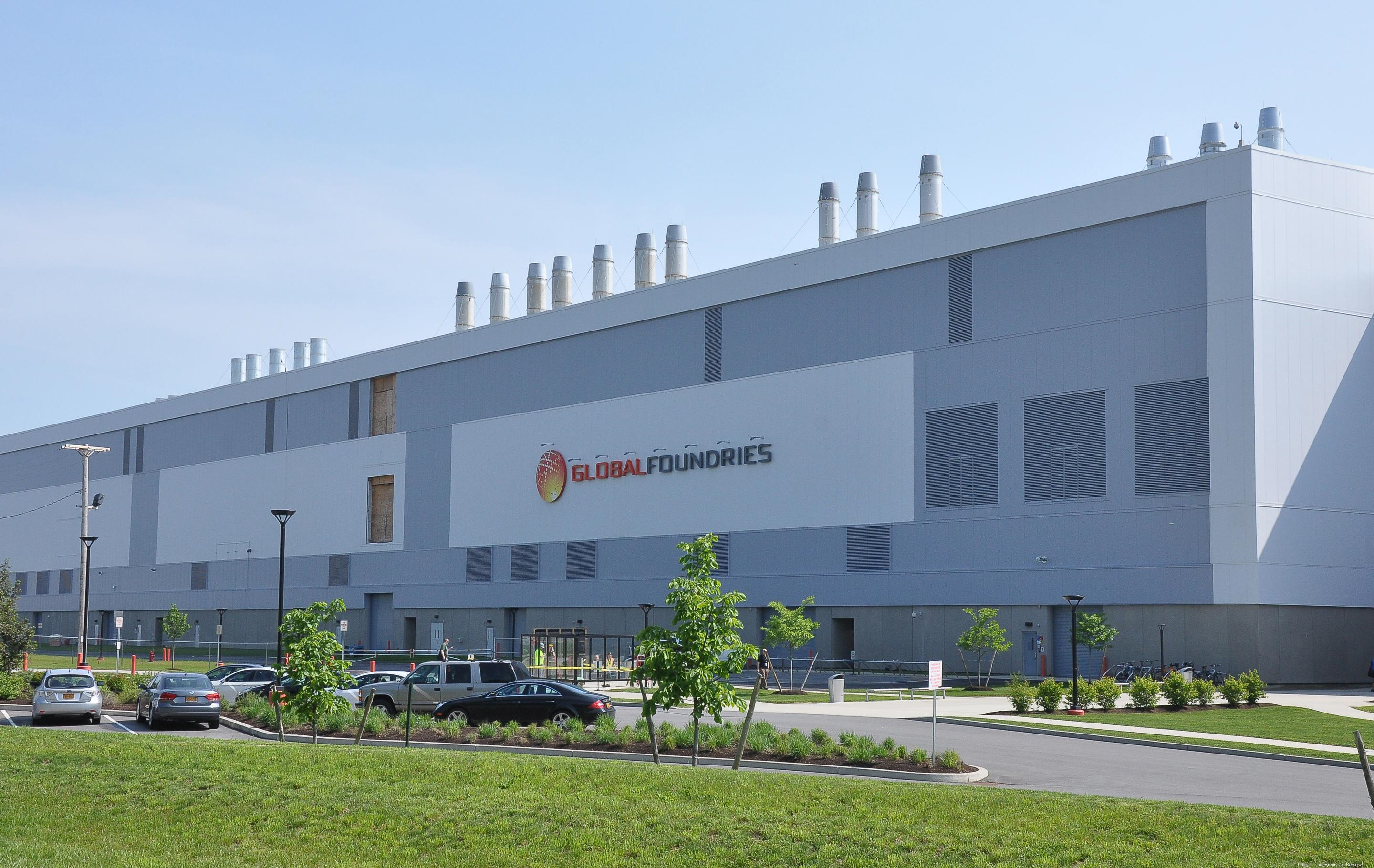 GlobalFoundries Fab 8. Photo by FinanceFeeds.net
After the latest expansion in 2013, the Fab 8’s capacity is around 60,000 wafer starts per month. The exact capacity today depends on several factors because the company now processes wafers using a more advanced process technology (the 14LPP) that uses multi-patterning, which effectively reduces capacity because each wafer spends more time in the cleanroom. In a bid to increase the output of 14LPP FinFET ICs by 20% by early 2018, the company intends to boost its production capacity. The firm said that the expansion does not involve physical expansion of the cleanroom, but the installation of additional more advanced step-and-scan systems and/or other tools into the existing space. For example, a switch from the TWINSCAN NXT:1960Bi to the TWINSCAN NXT:1980Di increases output of wafers by around 20% as the latter can process 275 wafers per hour versus 230 wafers per hour.
As the company is preparing to start high-volume manufacturing (HMV) of chips using its 7 nm FinFET technology in the second quarter of next year (so, several months ahead of the plan), the actual output of the Fab 8 remains to be seen. Initially, GlobalFoundries plans to use deep ultraviolet (DUV) lithography with quadruple patterning to produce chips using its 7 nm process, but sometime in 2019 it intends to start using extreme ultraviolet (EUV) lithography for a new wave of 7 nm designs. Usage of EUV will not eliminate multi-/quadruple-patterning, but will be used for cirical layers and will thus help to increase output of leading-edge chips. At present, the company does not talk about its 7 nm capacity, but it is logical to assume that the current expansion will have a positive effect on it as well.
In fact, the expansion of the Fab 8 is important for the fabless semiconductor industry as a whole because there are not a lot of foundries capable of producing ICs using FinFET manufacturing technologies. While numerous companies (like TowerJazz and Vanguard) ceased to develop leading-edge fabrication processes quite some time ago, SMIC and UMC are struggling with FinFETs as well. Moreover, neither of them are adopting FD-SOI-based planar technologies. As a result, there are only three pure-play foundries to offer HMV FinFETs to fabless chip designers: GlobalFoundries, Samsung Foundry and TSMC (Intel's 10nm ARM Artisan IP foundry business is potentially to add to that list in due course). Besides, there are two companies to offer advanced FD-SOI-based planar technologies: GF and Samsung.
Fab 1 Gets More FD-SOI
Fab 1 used to be AMD’s flagship production facility and it remains GlobalFoundries’ highest-capacity plant that can process up to 80,000 wafers per month. While it does not produce chips using the most advanced technologies with FinFETs, it is used to make energy-efficient ICs using low-power and cost-optimized planar FD-SOI-based manufacturing processes. Since the development of FinFET-based chips costs significantly more than the development of ICs with planar transistors, planar process technologies continue to make sense for many designers of chips (especially smaller ones). To fulfill demand from such customers developing ICs for Internet of Things (IoT), smartphone, automotive electronic and other applications, GlobalFoundries plans to expand the capacity of the Fab 1 by 40% by 2020 (it is only going to expand the FD-SOI lines). GlobalFoundries did not elaborate whether the expansion involves the construction of new buildings, the physical increase of the cleanroom space of one (or both) of the two fab modules or installation of new equipment.
At present, the company offers a variety of planar manufacturing processes at Fab 1, including various 28 nm bulk technologies as well as its FD-SOI 22FDX (it uses back-end-of-line interconnect flow of STMicroelectronics’ 28nm FD-SOI, as well as front-end-of-line STM’s 14nm FD-SOI process technology). GlobalFoundries pins a lot of hopes on the FD-SOI technology and the significant expansion of the Fab 1 re-emphasizes this commitment.
The expansion of the factory will help to boost not only 22FDX output, but could also offer significant production capacities for developers designing for the next-gen FD-SOI technology, 12FDX (we do not say that all of the new equipment will be re-used for the 12FDX, but at least some tools will be). GlobalFoundries does not release too many details about the 12FDX process to the public, but it says that it enables “the performance of 10 nm FinFET with better power consumption and lower cost than 16nm FinFET,” while also offering a 15% geometry scaling benefit compared to “today’s FinFET technologies” (if by “today’s” GF means 14LPP and CLN16FF/FF+, then the 12FDX has a 15% higher transistor density compared to technologies based on 20 nm BEOLs). The company expects the first 12FDX tape-outs in the first half of 2019, so the expansion of the Fab 1 by 2020 will likely be a benefit for FD-SOI designers in general.
The First Fab in China
Meanwhile, GlobalFoundries’ FD-SOI efforts will not be limited to its Germany manufacturing facility (even though the Fab 1 will remain the key development site for the tech). The company’s first fab in China (which might be called the Fab 11, but we will call it the Chengdu fab for now) will also be able to produce chips using the 22FDX. But before jumping to the FD-SOI in China, let’s talk about the plant itself first.
The Chengdu fab will be built in a partnership between GlobalFoundries and the Chengdu municipality. The first phase of the fab will begin operations in 2018 and it will use mainstream 180/130 nm fabrication technologies. The fab will initially process around 20,000 wafers per month. It is important to note that the mainstream manufacturing technologies that the Chengdu fab will use were originally developed by Chartered and not by AMD for its CPUs. The second phase will start operations in 2019 and will eventually be able to process 65,000 wafers per month using the 22FDX technology.
When fully ramped, the Chengdu fab will have a capacity of approximately 1,000,000 wafers per year (so, around 83,000 ~ 85,000 wafers per month for the phase 1 and phase 2 when both are fully operational) and will be a tangible manufacturing asset for GlobalFoundries. The fab is meant to fulfill increasing demand from China-based developers of semiconductors, but it will also be used to make chips for other fabless companies using primarily the 22FDX process, further increasing FD-SOI manufacturing capacities of GlobalFoundries and making the tech more attractive to customers requiring very high product volumes.
It is noteworthy that one of the interested parties in GF’s 22FDX tech is Rockchip, which has so far used only bulk process technologies of TSMC, SMIC and GlobalFoundries to produce its mobile SoCs. Other adopters of FD-SOI are developers of various wireless chips (like modems) and ICs that have to be very energy-efficient (particularly in idle mode).
Singapore Fabs Get a Boost
Finally, in addition to expanding the leading edge Fab 1 and Fab 8 as well as building a new semiconductor manufacturing facility, GlobalFoundries intends to increase the output of its fabs in Singapore.
The company does not publish too many details about the Singapore expansion, but only says that it intends to increase 40 nm capacity at its 300-mm Fab 7 by 35% and also boost output of its lines processing wafers using its 180 nm manufacturing process. Furthermore, GlobalFoundries will install new tools to make chips using its RF-SOI fabrication tech presumably on 300 mm wafers (which may be a big deal).
The Right Capacity at the Right Time
Since modern fabs and production tools cost billions of dollars to build, semiconductor manufacturers typically cannot afford them standing idle. A lack of capacity means that foundries cannot land orders from customers and eventually lose market share to rivals. Therefore it is important to have the right capacity and process technologies at the right time.
According to IC Insights, sales of all pure-play foundries in 2016 totaled around $50 billion, growing 11% year-over-year. GlobalFoundries was the second largest contract maker of chips with an estimated $5.5 billion in revenue (keep in mind that the company does not officially comment on such numbers), up 10% YoY. In a bid to sustain growth, GlobalFoundries needs to gradually increase its production capacities and the installation of new tools will serve the purpose, just like building a new fab in China.
For foundries, expanding production capacities is a usual business and they always try to optimize their output to meet demands from customers. GlobalFoundries is selectively adding capacities to popular nodes (and companies like MediaTek, Qualcomm, and Rockchip have already welcomed the decision), which is a smart move. In addition, it plans to build a new fab in China, which is a clever way to address a particular territory.
Related Reading:
Source: GlobalFoundries


49 Comments
View All Comments
psychobriggsy - Monday, February 13, 2017 - link
Well we know one thing: 8MB L3 SRAM on Intel is 19mm^2, 8MB L3 SRAM on AMD is 16mm^2.It's unlikely that they differ in much in configuration, it's either 6T or 8T SRAM for both of them, given the frequencies it has to run at (we do have some evidence that Intel's L3 SRAM throttles at a certain level though, maybe AMD's will too, we'll find out).
BurntMyBacon - Monday, February 13, 2017 - link
@psychobriggsy: "Well we know one thing: 8MB L3 SRAM on Intel is 19mm^2, 8MB L3 SRAM on AMD is 16mm^2.It's unlikely that they differ in much in configuration, ..."
http://www.eetimes.com/document.asp?doc_id=1331317...
Standard 6t SRAM
Zen - 0.0806mm^2
Competitor A - 0.0588mm^2
Given Zen's standard 6t SRAM is 37% larger than Competitor A's (Skylake), I'd say it is in fact very likely that they differ in configuration. There is almost certainly a design trade-off going on here and we'll have to wait and see whether Intel or AMD made the smarter trade-off. That does not. however, make the processes equal. All feature sizes listed in the chart are smaller on the Intel process (CPP, Fin Pitch, Metal Pitch, and 6t SRAM).
That all said, process advantage doesn't have the same meaning that it once did. The power advantage is offset somewhat by higher leakage as transistors get smaller. The frequencies seem to have hit a brick wall. The space (cost) savings are offset a fair bit by the more expensive processes and poor yields. Sure, it can be painful being several processes behind (See AMD FX series), but one or a half node behind isn't nearly so meaningful.
Wilco1 - Sunday, February 12, 2017 - link
Well you replied to a post that suggested that AMD was catching up - "closing the gap", so "only comparable" suggests that GF 7nm is still worse than Intel 10nm when in reality it is leap frogging Intel by 30%. And if Intel is as slow with rolling out 7nm as it was with 10nm, GF will enjoy that lead for several years.There is no point in comparing 7nm to 7nm given that Intel will be last with 7nm. So who has the best (densest) process right now? Today both Samsung/TSMC are well ahead of Intel. Later this year Intel and TSMC will be almost equal. That's the reality.
BurntMyBacon - Monday, February 13, 2017 - link
If I'm reading that correctly, the chart shows Intel 10nm = TSMC 7nm and Intel 7nm = TSMC 5nm. They are not just close, they are right on top of each other. That said, there are a lot more physical size features to compare than just metal pitch and poly pitch. Beyond size, there are also doping consistency across the wafer, power leakage (combination of individual element properties), defect rate, and a large list of other intrinsic properties that differ between processes and can make one process more desirable than another. For example, the Apple A9 SoC is dual source from TSMC (16nm) and Samsung (14nm). Despite being marginally larger on the TSMC 16nm node, the chip apparently has (marginally?) better power characteristics than the Samsung equivalent. Samsung has since released an updated 14nm node that likely eliminates or possibly even reverses the disparity.SaturnusDK - Saturday, February 11, 2017 - link
If you mean in terms of not existing in a product yet... you're rightvladx - Saturday, February 11, 2017 - link
Everyone wants to delay the inevitable, not just Intel or GF.Nagorak - Sunday, February 12, 2017 - link
That's what has been claimed, but if AMD is really catching up to Intel with Ryzen, then it's not looking like it's accurate. Supposedly Intel's 14nm is also better, but then how can Ryzen be on par (granted we haven't seen it yet). I say if Ryzen is basically on-par with Sky Lake then the process advantage will be revealed to be false. And if Intel has lost the process advantage they could be in for a rough time.psychobriggsy - Monday, February 13, 2017 - link
In some aspects, maybe. But Intel's 14nm has its own quirks. In the end, it appears that GF 14nm and Intel 14nm at a die level gain similar overall achieved transistor densities. Intel has smaller transistors, GF has many 2D low level metal layers that enabled better packing of their larger transistors.Robert Pankiw - Saturday, February 11, 2017 - link
I understand that a larger node can mean cost savings for clients not needing the most cutting edge technology, and as the author mentioned somewhere, it is easier to make planar than it is to make finfet. I can't find the exact quote on my phone. But what gets me is making a new fab on 180/130nm. Surely a smaller node, but still planar, would be better. More chips per wafer must mean more capacity and higher revenue, not to mention the benefits to the client of getting something more energy efficient. What is it that I am not quite getting?Disclaimer: I am not in any way deeply knowledgeable about this industry. I don't even know what many of the acronyms mean.
vladx - Saturday, February 11, 2017 - link
Because there's a lot of stuff like embedded ICs, sensors and probably even industrial robots and PLCs running on 130/180nm nodes. Not every device in the computing world needs the latest tech available.