Western Digital Announce BiCS4 3D NAND: 96 Layers, TLC & QLC, Up to 1 Tb per Chip
by Anton Shilov on June 28, 2017 10:00 AM EST
Western Digital on Tuesday formally announced its fourth-generation 3D NAND memory, developed as part of the Western Digital/Toshiba joint venture. The fourth-generation BiCS NAND flash chips from Western Digital feature 96 layers and will include several capacity points and will use TLC and QLC architectures. The company expects to start volume production of BiCS4 chips in 2018.
NAND dies that belong to the fourth-generation BiCS 3D NAND will use 96 word layers to minimize die size of the chips and maximize output of fabs, and at this point represents the largest layer count in the flash memory industry. Furthermore the range of BiCS4 NAND die configurations available will be considerably more diverse than BiCS3, which currently only includes 256 Gb and 512 Gb dies. Western Digital plans to offer BiCS4 components based on TLC (triple level cell) and QLC (quadruple level cell) configurations. with capacities ranging from 256 Gb to 1 Tb.
It is noteworthy that Western Digital’s BiCS4 lineup will include QLC NAND, which has been discussed by Western Digital (and SanDisk before that) for several years, but which is about to become reality only in the coming quarters. To store four bits per cell (with 16 voltage states) Western Digital had to use a “thick” process technology alongside multi-layer 3D NAND to keep the per-bit costs down. The company is not specifying how many program/erase cycles its 3D QLC NAND will handle, but various industry predictions over the years have suggested 100 – 150 P/E cycles as a reasonable goal for QLC NAND, which is considerably lower than approximately 1000 P/E cycles supported by TLC NAND. Given such endurance, it is logical to expect 3D QLC NAND to be used for primarily removable storage as well as for ultra-high capacity datacenter drives for the so-called near-WORM (write once read many) storage applications. For example, Toshiba last year discussed a QLC-based datacenter SSD with 100 TB capacity for WORM apps.
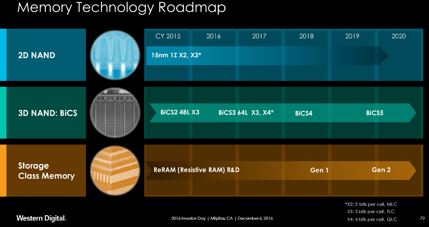
Western Digital plans to begin sampling of select 96-layer BiCS4 3D NAND configurations in the second half of this year, but the manufacturer does not specify which dies will sample when. As for mass production, Western Digital intends to start volume manufacturing of their 96-layer 256 Gb 3D NAND in 2018, with other dies to follow later. Based on Western Digital’s announcements made earlier, the company will gradually introduce more sophisticated BiCS4 96-layer configurations in 2018 and 2019, before moving to BiCS5 sometimes in 2020. That said, it makes sense to expect the highest capacity BiCS4 ICs to ship later rather than sooner.

Finally, Western Digital did not disclose whether it uses NAND string stacking technology to assemble its 96-layer 3D NAND dies, but it is a likely scenario given what industrial publications have been predicting.
Related Reading:
Source: Western Digital


22 Comments
View All Comments
MrSpadge - Wednesday, June 28, 2017 - link
Data retention time is usually 1 year for consumer flash. I recently had a USB stick in my car at somewhat elevated temperatures. The music was heavily corrupted after ~14 months. You'll definitely want the controler to read and refresh the data before you loose those few electrons comprising each bit, i.e. you'll need more write endurance than that. There are definitely applications where 100 - 150 cycles are perfectly fine, though.Personally I have never worn out any USB stick or flash card.Alexvrb - Wednesday, June 28, 2017 - link
They would not be good for a primary/sole drive, but I see them as potential replacements for mechanical mass storage drives. Something like NVMe for primary, QLC for storage. I would still like to see those figures come up before I use one. But even with low P/E ratings, as secondary storage they would still very likely be more reliable than typical consumer grade mechanical drives. They also won't make any noise during use.This is all down the road anyway. We'll see.