Big Volta Comes to Quadro: NVIDIA Announces Quadro GV100
by Ryan Smith on March 27, 2018 1:30 PM EST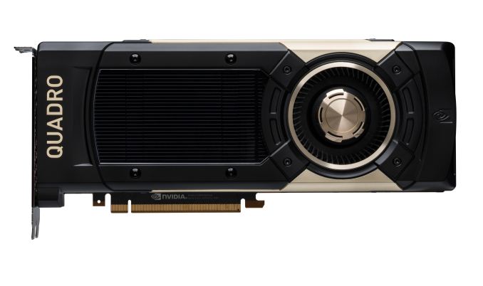
Along with today’s memory capacity bump for the existing Tesla V100 cards, NVIDIA is also rolling out a new Volta-based card for the Quadro family. Aptly named the Quadro GV100, this is the successor to last year’s Quadro GP100, and marks the introduction of the Volta architecture into the Quadro family.
As a consequence of NVIDIA’s GPU lines bifurcating between graphics and compute, in the last couple of years the Quadro family has been in an odd spot where it straddles the line between the two. Previously the king of all NVIDIA cards, instead the Quadro family itself has been bifurcated a bit, between the compute GPU-derrived cards like the Quadro GP100 and now GV100, and the more pure graphics cards like the P-series. The introduction of the Quadro GV100 in turn looks to maintain status quo here, delivering an even more powerful Quadro card with chart-topping graphics performance, but also the GV100’s GPU’s strong compute heritage.
| NVIDIA Quadro Specification Comparison | ||||||
| GV100 | GP100 | P6000 | M6000 | |||
| CUDA Cores | 5120 | 3584 | 3840 | 3072 | ||
| Tensor Cores | 640 | N/A | N/A | N/A | ||
| Texture Units | 320 | 224 | 240 | 192 | ||
| ROPs | 128 | 128 | 96 | 96 | ||
| Boost Clock | ~1450MHz | ~1430MHz | ~1560MHz | ~1140MHz | ||
| Memory Clock | 1.7Gbps HBM2 | 1.4Gbps HBM2 | 9Gbps GDDR5X | 6.6Gbps GDDR5 | ||
| Memory Bus Width | 4096-bit | 4096-bit | 384-bit | 384-bit | ||
| VRAM | 32GB | 16GB | 24GB | 24GB | ||
| ECC | Full | Full | Partial | Partial | ||
| Half Precision | 29.6 TFLOPs? | 21.5 TFLOPs | N/A | N/A | ||
| Single Precision | 14.8 TFLOPs | 10.3 TFLOPs | 12 TFLOPs | 7 TFLOPs | ||
| Double Precision | 7.4 TFLOPs | 5.2 TFLOPs | 0.38 TFLOPs | 0.22 TFLOPs | ||
| Tensor Performance | 118.5 TLFOPs | N/A | N/A | N/A | ||
| TDP | 250W | 235W | 250W | 250W | ||
| GPU | GV100 | GP100 | GP102 | GM200 | ||
| Architecture | Volta | Pascal | Pascal | Maxwell 2 | ||
| Manufacturing Process | TSMC 12nm FFN | TSMC 16nm | TSMC 16nm | TSMC 28nm | ||
| Launch Date | March 2018 | March 2017 | October 2016 | March 2016 | ||
While NVIDIA’s pre-brief announcement doesn’t mention whether the Quadro GP100 is being discontinued, the Quadro GV100 is none the less the de facto replacement for NVIDIA’s last current-generation Big Pascal card. The official specifications for the card put it at 14.8 TFLOPs of single precision performance, which works out to a fully-enabled GV100 GPU clocked at around 1.45GHz. This is only a hair below the mezzanine Tesla V100, and ahead of the PCIe variant. And like the capacity-bumped Tesla cards, the Quadro GV100 ships with 32GB of natively ECC-protected HBM2. This finally gets an NVIDIA professional visualization card to 32GB; the GP100 was limited to 16GB, and the Quadro P6000 tops out at 24GB.
On the features front, the card also ships with NVIDIA’s tensor cores fully enabled, with performance again in the ballpark of the Tesla V100. Like the Quadro GP100’s compute features, the tensor cores aren’t expected to be applicable to all situations, but there are some professional visualization scenarios where NVIDIA expects it to be of value. More importantly though, the Quadro GV100 continues the new tradition of shipping with 2 NVLink connectors, meaning a pair of the cards can be installed in a system and enjoy the full benefits of the interface, particularly low latency data transfers, remote memory access, and memory pooling.
At a high level, the Quadro GV100 should easily be the fastest Quadro card, a distinction the GP100 didn’t always hold versus its pure graphics siblings, and that alone will undoubtedly move cards. As we’ve already seen with the Titan V in the prosumer space – NVIDIA dodging expectations by releasing the prosumer Volta card first and ProViz card second – the Titan V can be a good deal faster than any of the Pascal cards assuming that software is either designed to take advantage of the architecture, or at least meshes well with NVIDIA’s architectural upgrades. Among other things, NVIDIA is once again big into virtual reality this year, so the GV100 just became their flagship VR card, a convenient timing for anyone looking for a fast card to drive the just-launched HTC Vive Pro.

However the GV100’s bigger calling within NVIDIA’s ecosystem is that it’s now the only Quadro card using the Volta architecture, meaning it’s the only card to support hardware raytracing acceleration, vis a vie NVIDIA’s RTX technology. Announced last week at the 2018 Game Developers Conference, RTX is NVIDIA’s somewhat ill-defined hardware acceleration backend for real-time raytracing. And while the GDC announcement was focused on the technology’s use in games and game development, at GTC the company is focusing on the professional uses of it, including yet more game development, but also professional media creation. Not that NVIDIA expects movie producers to sudden do final production in real-time on GPUs, but as with the game asset creation scenario, the idea is to significantly improve realism during pre-production by giving artists a better idea of what a final scene would look like.
Along with Microsoft’s new DirectX Raytracing API, the RTX hardware will also be available within NVIDIA’s OptiX ray tracing engine – which is almost certainly a better fit for ProViz users – while NVIDIA is also saying that Vulkan support is on tap for the future. And like the game development scenario, NVIDIA will also be looking to leverage their tensor cores here as well in order to use them for AI denoising. Which, given the still limited raytracing performance of current hardware, is increasingly being setup as the critical component for making real-time ray tracing viable in 2018.
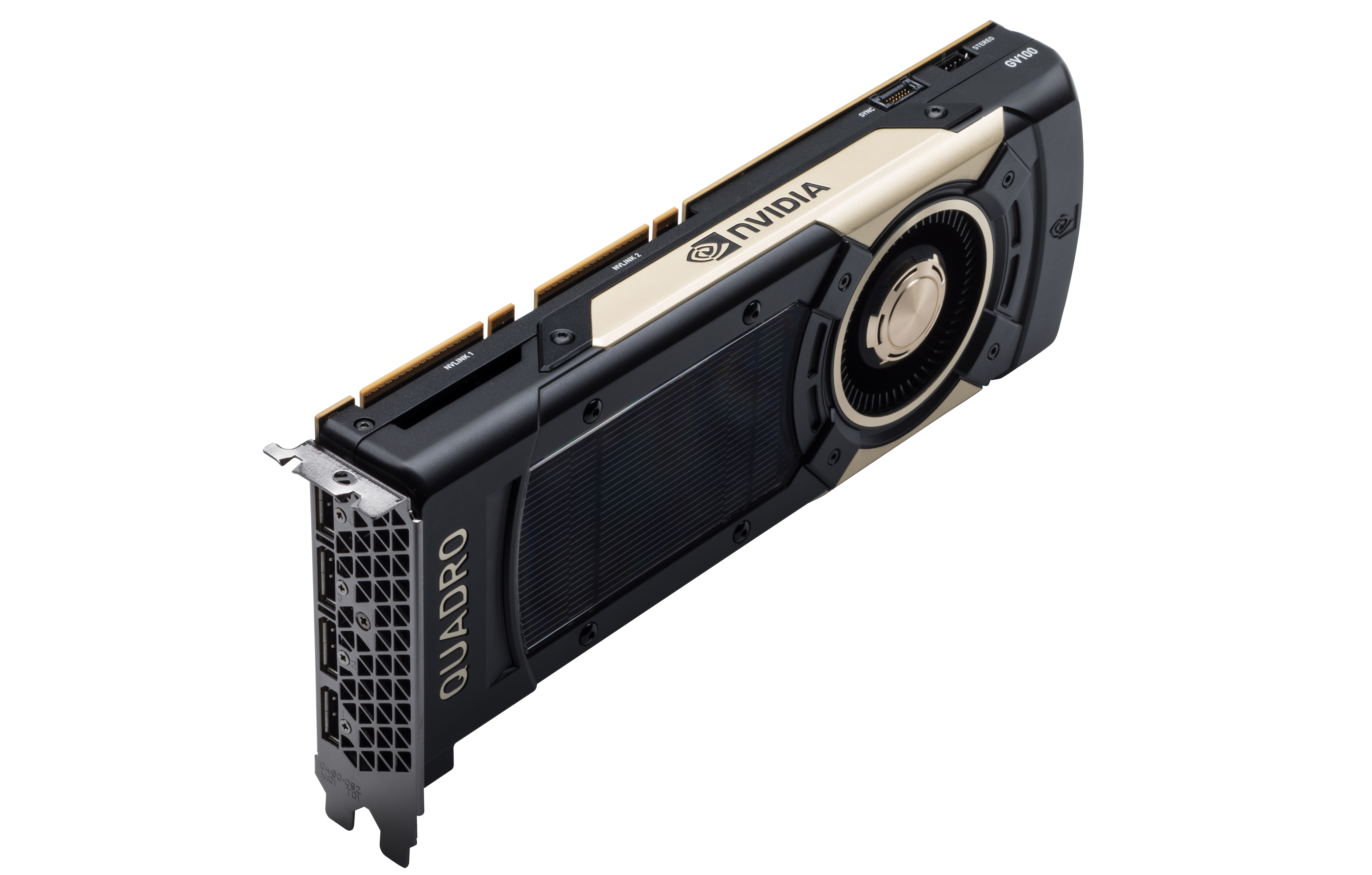
Otherwise, the Quadro GV100 looks to be a fairly standard Quadro card. TDP has gone up ever slightly from the Quadro GP100 – from 235W to 250W – so while it should generally be drop-in replaceable, it’s not strictly identical. Nor are the display outputs identical; the Quadro GV100 has dropped the GP100’s sole DVI port, leaving it with a pure 4x DisplayPort 1.4 setup. The card also features the standard Quadro Sync and Stereo connectors for synchronized refresh and quad-buffered stereo respectively.
Wrapping things up, the Quadro GV100 is shipping immediately from NVIDIA, and OEMs will begin including it in their systems in June. Official pricing has not been announced, but like the GP100 before it, I would expect this card to run for north of $5,000. Official pricing has also been announced for the card; NVIDIA's fastest Quadro will go for a cool $9,000.


21 Comments
View All Comments
mode_13h - Monday, April 2, 2018 - link
Not really. Your sense of scale is a muddled mess. There's no oscillation. PCs were never more powerful than mainframes. Cell phones were never more powerful than internet (or "cloud") servers.The trend went from mainframes -> PCs, as the issue was less about data and more about economically scaling processing power. Then, the internet came along and started the growth of datacenters. The rise of smartphones, globalization, and big data only accelerated this trend. Now, we live in an era of not "either or" but "both and". There's computing power both at the edge AND the core, and developers are able to shift the work to wherever it makes the most sense.
But, the reality is that if you need a lot of power in one device, it's going to be expensive. It has always been and always will be thus.
mode_13h - Monday, April 2, 2018 - link
I don't get why you're complaining. The high-end has always been out of reach of mere mortals. No reason to think that wouldn't continue.It's just that instead of being some IBM multi-core POWER CPU for mainframes, it's now Nvidia that has produced a GPU too big to be sold at a consumer price point. And you're no worse off for them having done so (except for the 12 nm manufacturing capacity being consumed by making it).
Instead of complaining about what you can't have, you can instead focus on what gains await consumers in the next few node shrinks of CPUs and GPUs.
Yojimbo - Tuesday, March 27, 2018 - link
The limit 5 per customer probably has more to do with overall supply shortage of the underlying GPU (GV100) and the HBM2 memory than with singling out any particular type of customer. It's the same GPU that is going into their high-end Tesla accelerators. The Titan-V (which also uses the GV100 and HBM2 memory) is out of stock, so it seems they can't build them fast enough to keep up with demand.Samus - Wednesday, March 28, 2018 - link
The ~120TFLOP tensor performance makes this thing quite competitive at 9k when you consider any other alternative would cost more.mode_13h - Monday, April 2, 2018 - link
Not competitive against Titan V.The only real distinguishing factors between the two are memory size and NVLink.
blppt - Tuesday, March 27, 2018 - link
Aha, finally, the GPU capable of running FFXV at 4k 60fps maxed out!Whats that? No game ready drivers? Bah.
Socius - Friday, March 30, 2018 - link
You can already do that with an overclocked Pascal Titan X.juhatus - Wednesday, March 28, 2018 - link
Tensor Performance 118.5 TLFOPsSurely TFLOPs
Luscious - Friday, March 30, 2018 - link
Reading between the lines here and it seems SLI on the Pascal generation was neutered for good reason. Those high bandwidth bridges just didn't work properly OR nVidia knew they would hit a wall with PCIe. NVLink was well under way by that point but if NVLink2 improves on it by being totally transparent from the software side (if what was said is correct) then that gives game developers a HUGE break when it comes to engine support.I can totally see NVLink2 replacing SLI on future gaming cards, probably under a new name like XLI. All nVidia needs to do is make 3/4 way NVLink bridges available (they may already have them). We all know they want to sell more cards to gamers, so they wouldn't say no to enthusiasts either who want two or more cards in their system, and very high end systems pushing 5K/8K panels.
mode_13h - Monday, April 2, 2018 - link
Your timeline is wrong. The *first* pascal chip had NVLink. They could've included it in the rest, if they'd wanted to. Then, they had another shot with Titan V, as it launched well after the V100-based Tesla products ushered in NVLink2. But Titan V didn't have it (enabled, at least).So, there's a clear pattern of Nvidia reserving NVLink for its workstation & datacenter products. Don't hold your breath for next gen SLI. I think they probably regard PCIe 3+ as adequate for multi-GPU gaming.