Arm's Cortex-A76 CPU Unveiled: Taking Aim at the Top for 7nm
by Andrei Frumusanu on May 31, 2018 3:01 PM EST- Posted in
- CPUs
- Arm
- Smartphones
- Mobile
- SoCs
- Cortex-A76
Another year, another TechDay from Arm. Over the last several years Arm’s event has come as clockwork in the May timeframe and has every time unveiled the newest flagship CPU and GPU IPs. This year is no exception as the event is back on the American side of the Atlantic in Austin Texas where Arm has one of its major design centres.
Two years ago during the unveiling of the Cortex A73 I had talked a bit more about Arm’s CPU design teams and how they’re spread across locations and product lines. The main design centres for Cortex-A series of CPUs are found in Austin, Texas; Cambridge, the United Kingdom, and Sophia-Antipolis in the south of France near Nice. For the last two years the Cortex A73 and Cortex A75 were designs that mainly came out of the Sophia team while the Cortex A53 and more recently the A55 were designs coming out of Cambridge. This means that we haven’t seen any recent designs coming out of Austin and the last of the “Austin family” of CPUs were the A57 and A72.
The project being worked on in Austin had been hyped up for several years – I remember even as early as the A73 release back in 2016 the company had pulled forward some elements from an advanced future microarchitecture on the back-end pipelines, especially on the FP/SIMD side. The Cortex A75 was further remarked as pulling more elements from this new mysterious project.
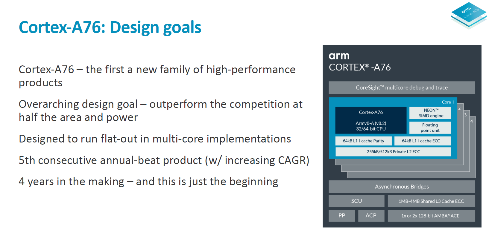
Today we can finally unveil what the Austin team has been working on – and it’s a big one. The new Cortex A76 is a brand new microarchitecture which has been built from scratch and lays the foundation for at least two more generations for what I’ll call “the second generation of Austin family” of CPUs.
The Cortex A76 is important for Arm for a design perspective as it represents a new start from a clean sheet. It’s rare for IP claim to be able to do this as it represents a great resource and time investment and if it weren’t for the Sophia design team taking over the steering wheel for the last two generations of products it wouldn’t have been reasonable to execute. The execution of the CPU design teams should be emphasised in particular as Arm claims this is the 5th generation “annual beat” product where the company delivers a new microarchitecture every new year. Think of it as an analogue to Intel’s past Tick-Tock strategy, but rather Tock-Tock-Tock for Arm with steady CAGR (compound annual growth rate) of 20-25% every generation coming from µarch improvements.
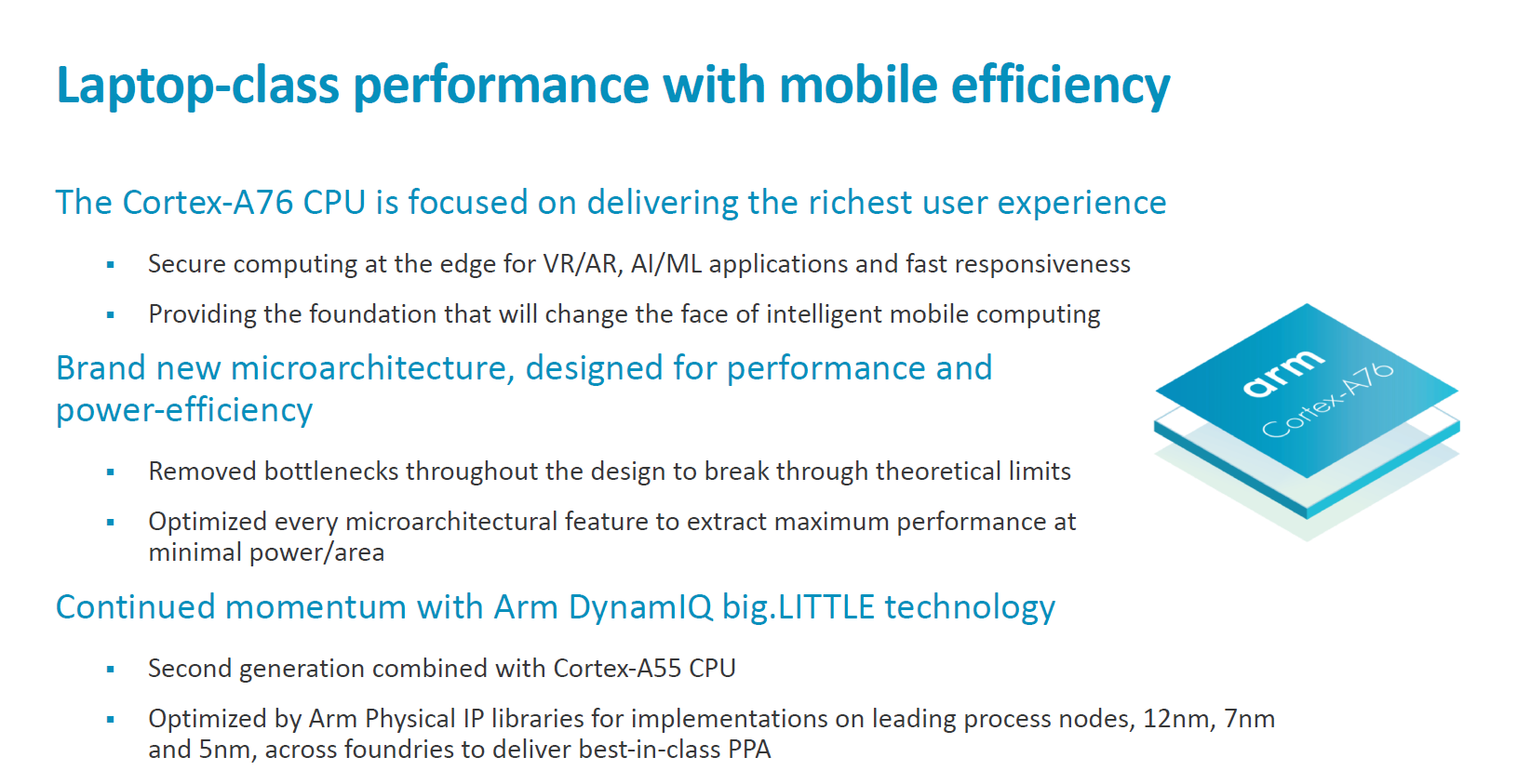
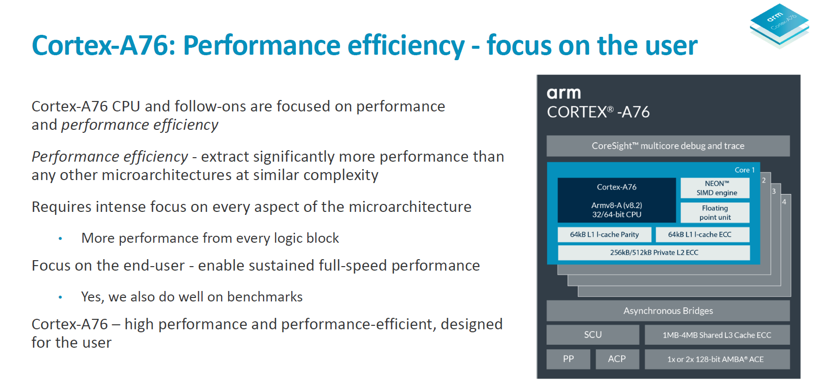
So what is the Cortex A76? In Arm’s words, it’s a “laptop-class” performance processor with mobile efficiency. The vision of the A76 as a laptop-class processor had been emphasised throughout the TechDay presentation so it seems Arm is really taking advantage of the large performance boost of the IP to cater to new market segments such as the emerging “Always connected PCs” which Qualcomm is spearheading with their SoC platforms.
The Cortex A76 microarchitecture has been designed with high performance while maintaining power efficiency in mind. Starting from a clean sheet allowed the designers to remove bottlenecks throughout the design and to break previous microarchitectural limitations. The focus here was again maximum performance while remaining within energy efficiency that is fit for smartphones.

In broad metrics, what we’re promised in actual products using the A76 is the follows: a 35% performance increase alongside 40% improved power efficiency. We’ll also see a 4x improvements in machine learning workloads thanks to new optimisations in the ASIMD pipelines and how dot products are handled. These figures are baselined on A75 configurations running at 2.8GHz on 10nm processes while the A76 is projected by Arm to come in at 3GHz on 7nm TSMC based products.
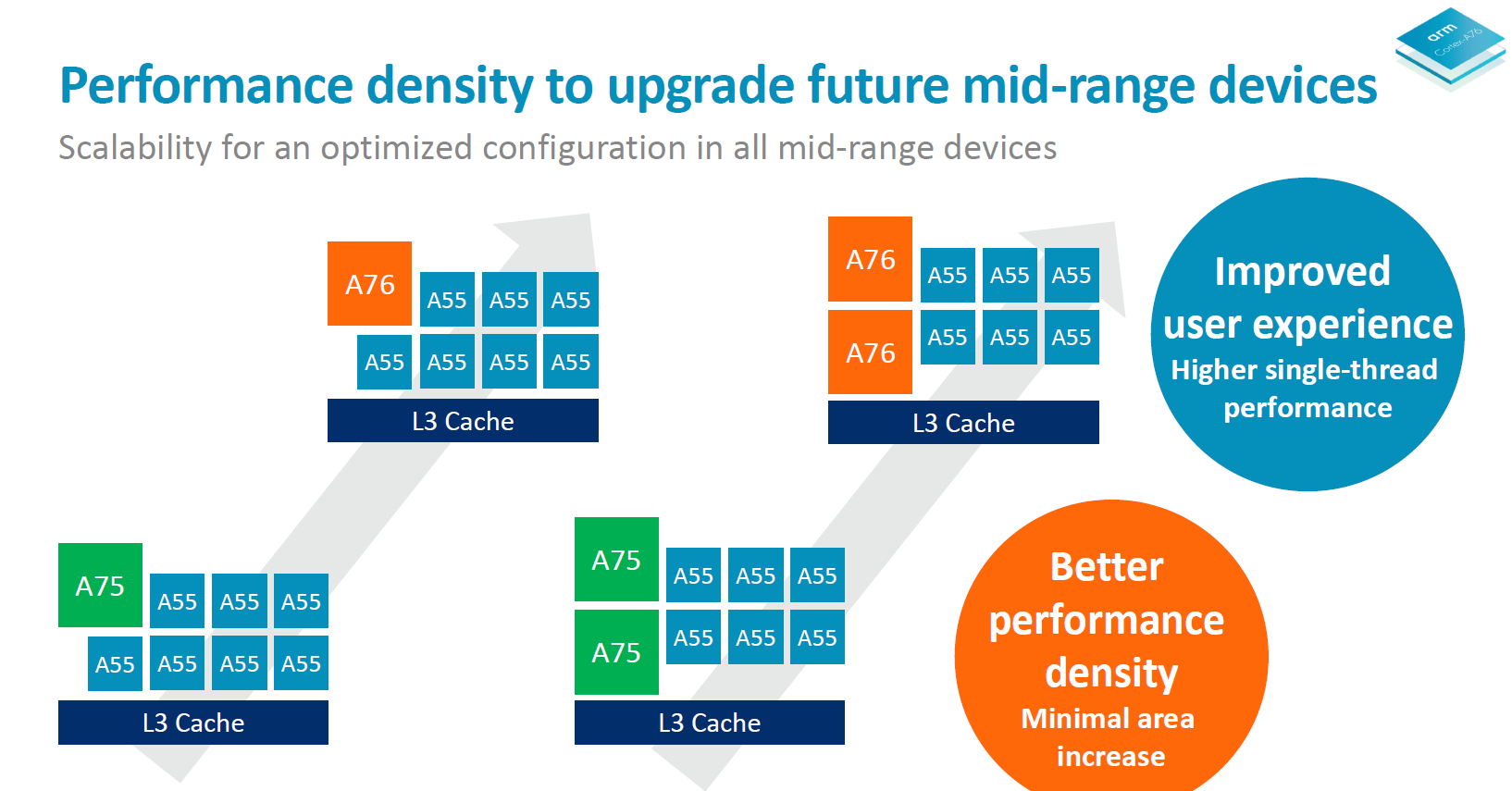
The new CPU is naturally still compatible with DynamIQ’s common cluster topology and Arm envisions designs to be paired with Cortex A55s as the little more power efficient CPUs. The configuration scalability of the DynamIQ IP again was reiterated and we were presented with example configurations such as 1+7 or 2+6 with either Cortex A75 or A76 CPU IP. This presentation slide was one of the rare ones where Arm referred to the area size of the A76, pointing out that the A75 still had better PPA and thus might still be a valid design choice for companies, depending on their needs. One comparison that was made during the event is that in terms of area, three A76’s with larger caches would fit inside the size of a Skylake core – all while within 10% of the IPC of the Intel CPU, but obviously there’s also process node scaling considerations to take into account.
A standout claim is that Arm aims to outperform the competition at half the area and half the power. Arm was slightly beating around the bush here in what it considers the competition, but generally the answer was that it was considering everybody the competition. Taking into account Intel, AMD or Samsung it’s actually not that hard to imagine Arm beating them in PPA as historically the company always had the smallest CPU designs and that directly translates into more efficient microarchitectures.
Before we get into more detailed breakdowns of the performance and power improvements and what I’m expecting to happen into products, let’s see the microarchitectural improvements on the core and how Arm managed to extract this much performance while maintaining power efficiency.


123 Comments
View All Comments
jospoortvliet - Wednesday, June 6, 2018 - link
Twice as fast at half power should not be hard. Of course the process has changed since those chips were baked, it isn't all in architecture.tipoo - Tuesday, September 4, 2018 - link
Yeah, on 7nm they should easily be able to make portable mode do what docked mode did, and add a new higher performance docked mode. Easy transition.name99 - Friday, December 18, 2020 - link
"The branch prediction unit is what Arm calls a first in the industry in adopting a hybrid indirect predictor. "This is somewhat misleading. The fetch unit is very interesting (and Andrei did not spend enough time praising it) but to say that it is first in the industry seems unreasonable.
The idea of decoupling the stream of fetch addresses from actual I-cache access dates from a thesis in 2001. Implementations I know about include Zen and Exynos M1 (2016) and IBM z14 (2017). Apple probably got in there even earlier.
So there may be some very specific detail in how ARM is implementing this that is a first, but the overall idea has been around for 17 years.
(The reason why it's taken so long to be implemented is that, first, it needs lots of transistors to store all the predictor state and, second, it requires some rethinking of how your branch predictors are indexed and updated. Think about it. What you want is machinery that, EVERY CYCLE, when given a PC will spit out two addresses -- where the current run of straightline fetching must end, ie the next TAKEN branch target, and where the PC must be directed to when it hits the end of this basic block. And it has to do this "in isolation", without looking at the instructions that are going to be loaded from the I$ because the whole point is that this is happening decoupled from, and in advance of, access to the I$. It's not trivial to think of a set of data structure that can do that. I'm still not at all convinced my understanding of exactly how this is correct, even though I've been trying to understand it for some time now.)