Samsung Begins Mass Production Of 96L 3D NAND
by Billy Tallis on July 9, 2018 11:00 PM EST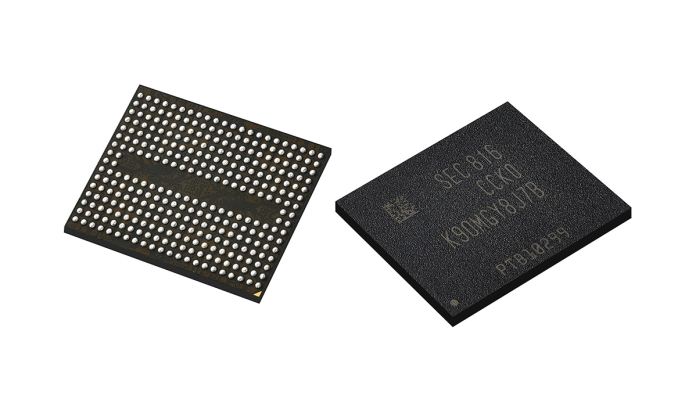
Samsung has started mass production of their fifth generation of 3D NAND flash memory, which they brand as V-NAND. This new generation bumps the layer count from 64 up to 96 (officially, "more than 90" layers), providing further density increases without incurring the endurance and reliability costs that came with process shrinks for planar NAND flash memory. Samsung first announced their 96L V-NAND at Flash Memory Summit in August 2017.
The fifth generation V-NAND also includes performance enhancements, most significantly a Toggle DDR 4.0 interface running at 1.4Gbps, compared to the 800Mbps interface speed of Samsung's previous 3D NAND. A reduction of operating voltage from 1.8V to 1.2V offsets the extra power consumption that faster interface speed would otherwise bring. Samsung is also citing improvements to both read and program latency. Read latency did not improve from 48L to 64L, but now has been "significantly" reduced to 50μs. Program (write) latency is down about 30% to 500μs.
Samsung hasn't shared many details about their process refinements, but the height of each memory cell layer has been reduced by 20%, which helps reduce the extremely high aspect ratio of the holes that need to be etched for the vertical strings of memory cells. Difficulties with high aspect ratio etching are widely believed to be the primary cause for delays that Samsung's 48L V-NAND suffered, which led to several product cancellations as Samsung's NAND development failed to keep pace with their SSD controller improvements. Samsung's transition to 64 layers was much smoother, and Samsung is claiming a 30% improvement to manufacturing productivity with the 96L process. Whether this is on a per-bit basis or a per-wafer basis, this should allow for another on-time roll out.
The first 96L part in mass production is a 256Gb TLC (three bits per cell) die, which should see broad usage in the mobile and SSD markets. Larger dies will follow to fulfill the need for higher capacities with lower cost per bit, primarily in the enterprise SSD market. This will include a 1Tb QLC NAND (four bits per cell) part.
Source: Samsung


25 Comments
View All Comments
Altimmons - Wednesday, July 11, 2018 - link
Then buy something else. It’s a free market after all. Unlike ram though I think the prices for storage are reasonable, affordable, and competitive. $200 for 500 Gb pro model. Not bad.gfkBill - Tuesday, July 10, 2018 - link
"20% for us, 10% for their margins and future R&D"Something like that, but don't forget their existing pricing has R&D and profit built in already, so no reason it can't be almost a 30% saving if it costs them 30% less to make it. Your 20% is probably pretty close to reality though.
Ultimately competition will dictate how much of a saving we actually see, more than anything. They'll cream it while they can, as first mover.
sleepeeg3 - Tuesday, July 10, 2018 - link
You are cursing Samsung for creating a better process? You have issues.Samsung competes with other companies so they can't arbitrarily charge more. Capacities will increase and price may come down. Everyone wins. That's the invisible hand of glorious capitalism.
Mikewind Dale - Thursday, July 12, 2018 - link
We have no right to expect that the cost savings will be transmitted direct to the consumer.First, the price that is charged is going to depend on what Samsung's competitors can charge. Samsung's incentive to offer a net sale (price plus performance) that is just slightly better than what their next best competitor can offer. If the price Samsung charges is too high, then blame their competitors. It makes no sense to blame an innovator who is offering something new. You should blame all their competitors who can't keep up.
Second, if savings in per-unit manufacturing costs were entirely transmitted to the consumer, then what would pay for the R&D? No company would ever engage in R&D unless it thought that it would keep some of the profits for itself. If every company transmitted all cost savings to the consumer, then there would never be any cost savings to begin with.
Atwork - Sunday, July 15, 2018 - link
If the new equipment they have to buy has a life-cycle cost that's 40% higher (not unexpected) then 30% higher "manufacturing productivity" (yield?) would make it a wash. Those FAB tools don't just cost millions to hundreds of millions each, most need to be refurbished or replaced after every x number of wafers are processed. Consumable costs are likely higher as well. Each layer requires a pass through each of several expensive tools. Each pass through each tool is a chance to trash a wafer, or layer - it's amazing they get 90 to 96 successful layers out of any wafer!bug77 - Tuesday, July 10, 2018 - link
Waiting to see how many p/e cycles these have left.Death666Angel - Tuesday, July 10, 2018 - link
"without incurring the endurance and reliability costs that came with process shrinks for planar NAND flash memory"bug77 - Tuesday, July 10, 2018 - link
Yes, additional stacks won't affect durability, but we don't know whether the other manufacturing parameters will remain unchanged.Mobile-Dom - Tuesday, July 10, 2018 - link
1.8v to 1.2v? damnCheapSushi - Tuesday, July 10, 2018 - link
Stoked about 96 layer QLC NAND for bulk storage.