Qualcomm Tech Summit, Day 3: Snapdragon 8cx, the New ACPC SoC
by Ian Cutress on December 6, 2018 5:35 PM EST- Posted in
- SoCs
- Snapdragon
- Qualcomm
- ACPC
- Snapdragon 8cx
- Qualcomm Summit 2018
For the final day of Qualcomm’s 3rd Annual Tech Summit, the focus is on its Always Connected PC (ACPC) platform. This is Qualcomm’s attempt to bring mobile processors to standard laptops by enabling Windows on Snapdragon devices. So far we have seen two generations of processors, both based on the preceding mobile chip for flexibility. Now Qualcomm has announced that the ACPC market will get its own dedicated chip, called the Snapdragon 8cx. Here’s what we know.
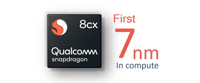
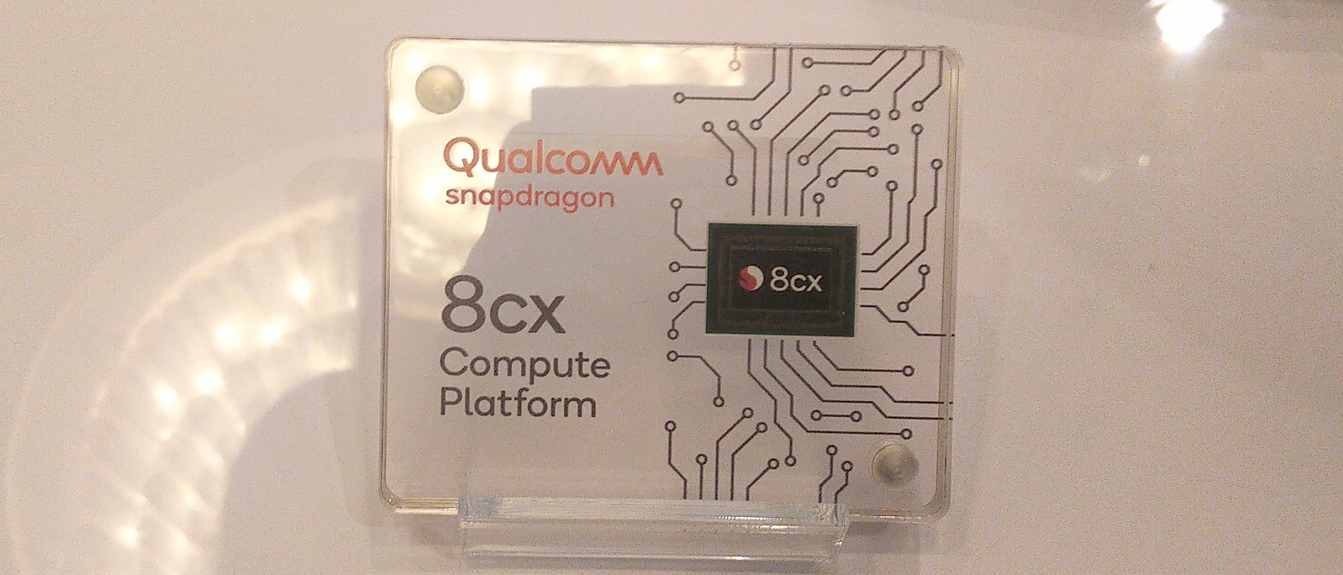
Snapdragon 8cx: World’s First Laptop 7nm SoC
The two previous ACPC chips from Qualcomm, the S835 and the S850, were simple enough to follow: put the mobile processor into a device that allows for higher power, but use the efficiency to extend battery life and the integrated modem to provide a smartphone-like always connected device. Rather than use Android, Qualcomm worked with Microsoft to enable a version of Windows that ran on the chips as well as working with software partners to enable their software on the device – for everything else, there’s an emulation layer if the software was built for x86 processors.
With this idea, Qualcomm was always reliant on two things: the most common software being natively supported, and for everything else efficient machine translation. The best way to speed either of those up is to use a more powerful processor, preferably one with a higher power budget and better efficiency point to squeeze the frequency out. This is what the Snapdragon 8cx is all about. Qualcomm stated that the 8cx will sit above the S850 in a new higher power category, rather than directly replace it.
For the name, c = Compute, and x = eXtreme. Just in case you were wondering.
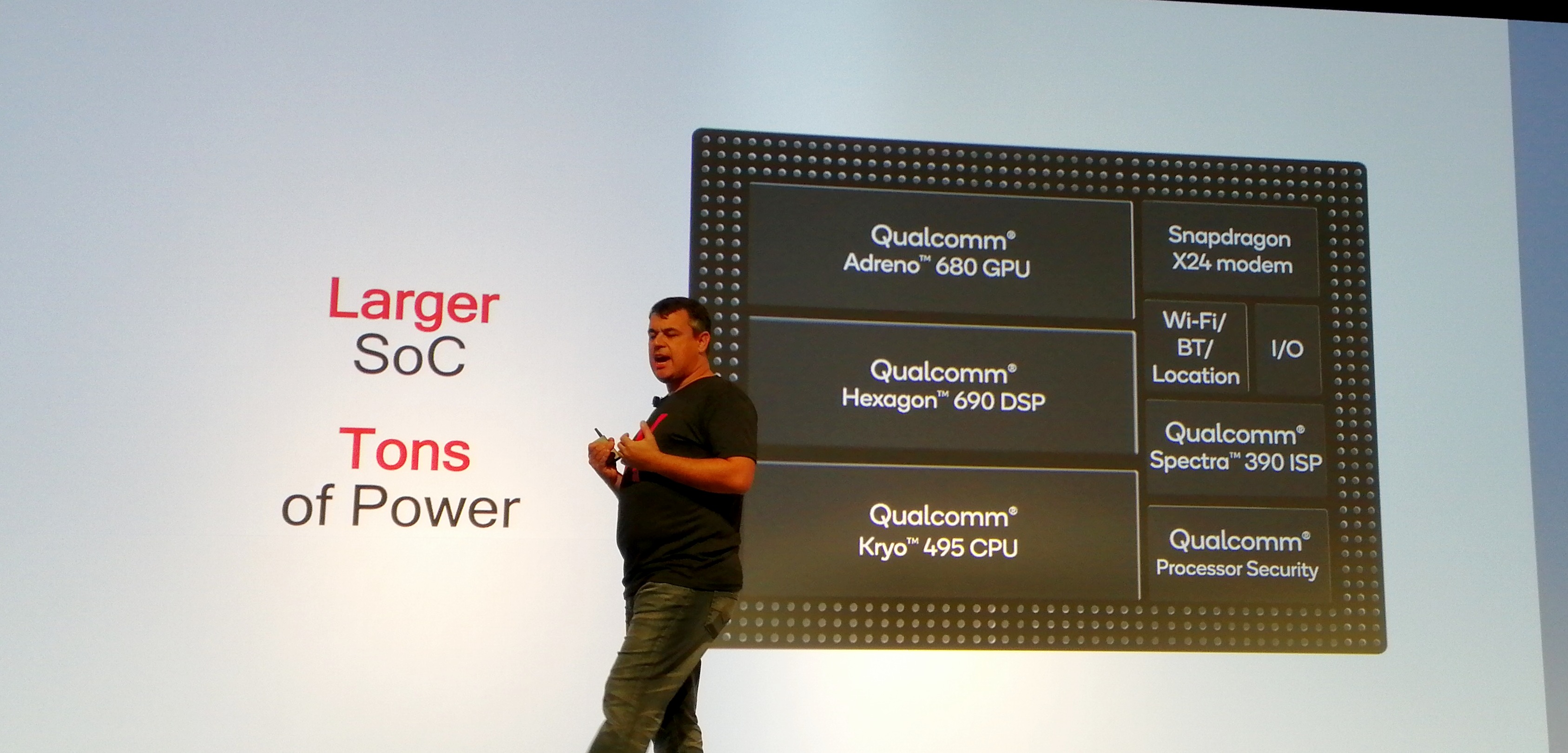
The new 8cx is built off of many of the same base elements as the Snapdragon 855 announced yesterday, but the 8cx is a larger chip with a number of key features expanded and enhanced for the intended market segments.
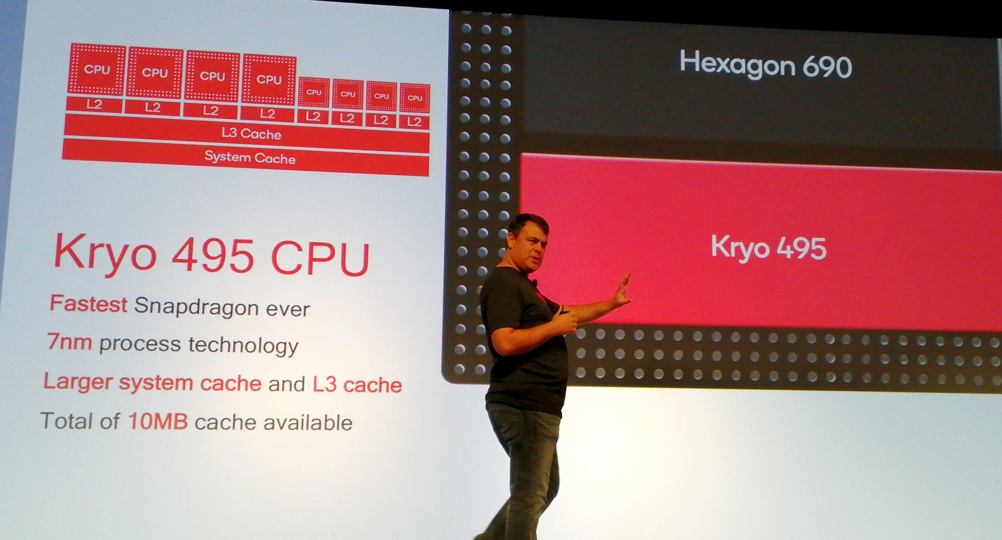
Starting with the CPU, this chip has eight next-generation Kryo 495 cores, split into four performance cores and four efficiency cores. Qualcomm states that these are the fastest Kryo cores the company has ever built, although at the time of writing the microarchitecture and frequencies have not been disclosed. (Update: the demo systems being used stated a peak big CPU speed of 2.75 GHz, although we were told by Qualcomm that the final speed will depend on the OEM implementation, so we're likely dealing with a configurable TDP.) We know that these cores are Arm v8.1-based, likely A76-variants designed under Arm’s program that offers some custom tweaking of the design for specific customers. In the presentation, Qualcomm stated that there is a total of 10 MB of cache, but doesn’t break it down into exactly where that cache is, however the system cache and L3 cache is listed as ‘larger’ than before.
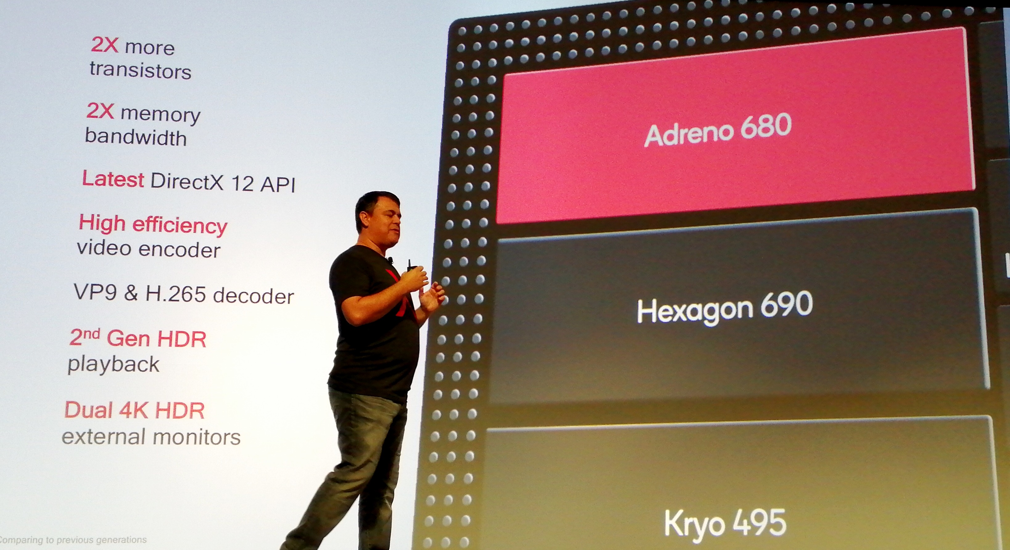
On the GPU, the new Adreno 680 graphics inside are only discussed in terms of performance metrics relative to previous platforms: we were told that the graphics are 2x faster than Snapdragon 850, 3.5x faster than the Snapdragon 835, and 60% more power efficient than the Snapdragon 850 (some of which will come from the process node). The new design was labelled as Qualcomm’s biggest leap in performance per watt in graphics technology ever, and that the Adreno 680 is Qualcomm’s most powerful GPU ever produced. This GPU also uses double the number of transistors of the previous generation.
Other headline features for the graphics includes support for the latest Vulkan 1.1 and DirectX 12 APIs, full VP9 and H.265 decode, a ‘high efficiency’ video encoder, and support for dual 4K HDR external displays.

Feeding the graphics is the memory, and Qualcomm is doubling the memory width for this new chip. Rather than a 64-bit wide interface, split as 4x16-bit channels, the Snapdragon 8cx will have a 128-bit wide interface, split as 8x16-bit channels. This interface will support up to 16GB of LPDDR4X, although at what speed we’re not sure. One of the criticisms of the previous generations of ACPC devices was the memory bandwidth – especially as Qualcomm’s competitors in this space routinely use 128-bit wide interfaces – so this should help tremendously both in day-to-day performance and in graphics performance.
The Snapdragon 8cx will support both UFS 3.0 storage and NVMe SSD storage, along with having an additional PCIe 3.0 x4 connection so OEMs can add external controllers. When I questioned Qualcomm if something like Thunderbolt 3 was possible, they said that they don’t see why it wouldn’t be if an OEM wanted to make that configuration.
Being built from mobile SoC principles means that the chip also has an integrated modem, and we get the Snapdragon X24 LTE modem similar to the S855 chip launched yesterday. This chip can support up to 2 Gbps download of LTE connectivity, using 7xCA and 4x4 MIMO on five of those streams. Peak upload speed is listed as 316 Mbps with 3x20 MHz CA. The 8cx will support 5G when the X50 modem is paired with it, however not much noise was mentioned on this given the 5G focus of the first day of the event. Beyond this is 802.11ac Wave support, although 802.11ax-ready support is not listed. Bluetooth 5.0 is also supported.
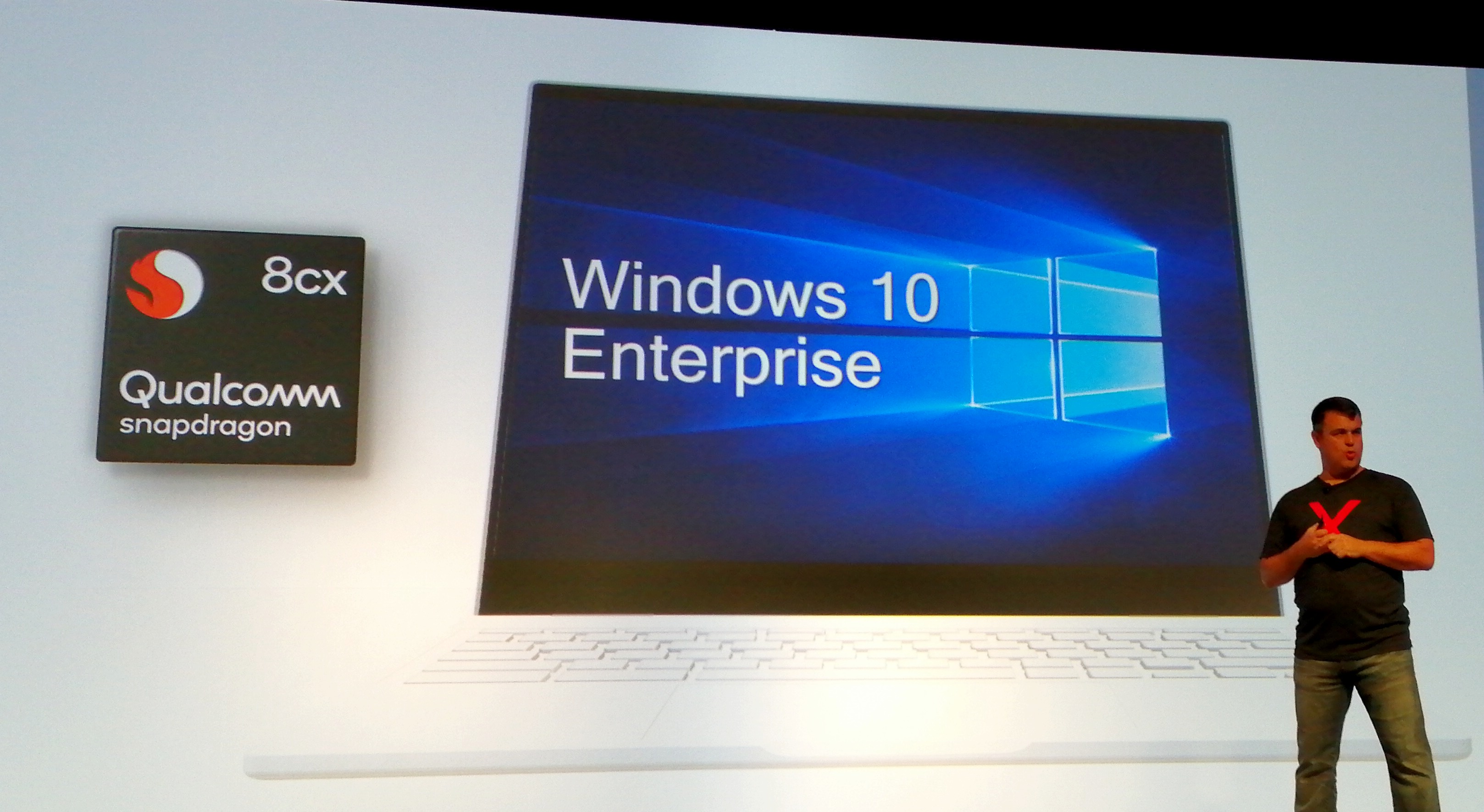
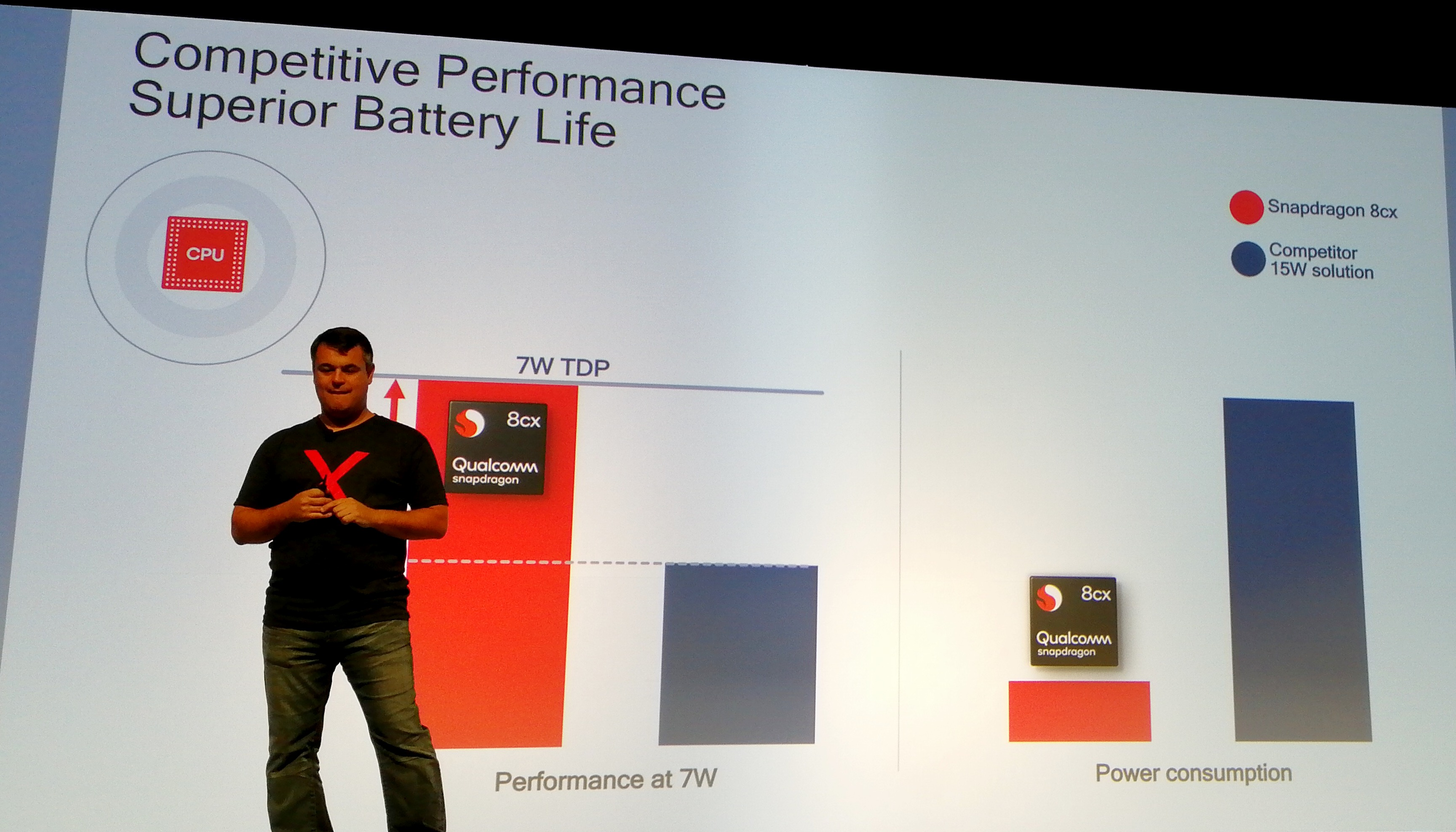
Qualcomm was very keen to announce full support for Windows 10 Enterprise, and expects the Snapdragon 8cx to push into the Enterprise/Commercial space given the focus on manageability and security that the OS provides. This is the proverbial shot across the bow of Intel’s commercial business, which sells millions of units every year. Qualcomm was keen to provide some performance and power numbers, symbolising better performance at 7W compared to Intel at a much lower power. No live demo was provided it should be said, but Qualcomm is making some bold claims that we're eager to check.
In the videos during the keynote presentation, a number of form factors were shown, including what looked like a Lenovo-based dual display unit and even a Surface like design. None of the partners on the stage were willing to discuss what their plans are for the Snapdragon 8cx right now, and the only inkling of an 8cx device we saw in the demo room was Qualcomm’s reference design, with the OEM they are using covered up.
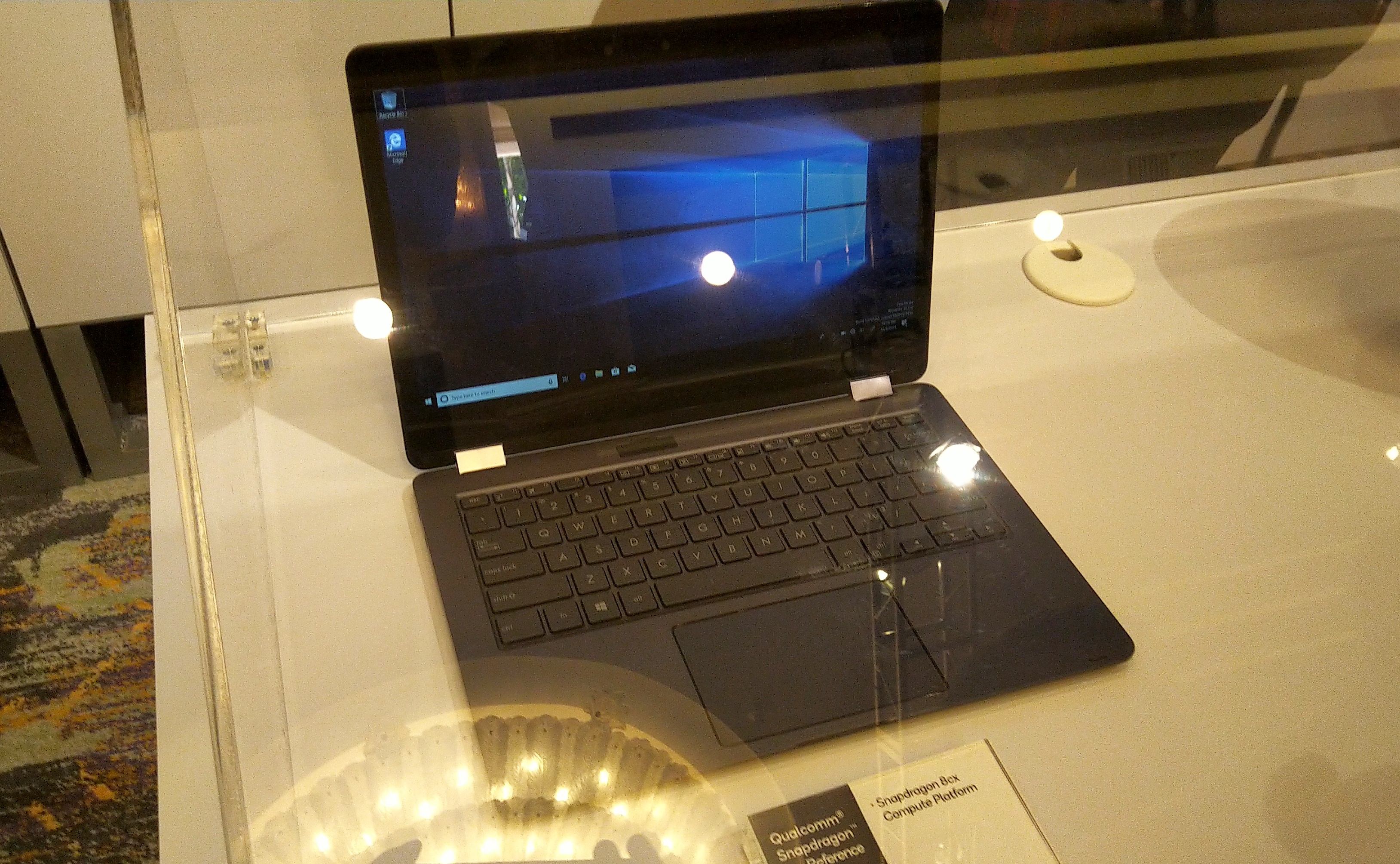
This looked like a common clamshell design, and Qualcomm stated that they will be rolling out these reference designs internally to employees (replacing their current mobile devices) as they put the final touches the firmware and software.
One of the key metrics for the ACPC market to succeed is software, and Qualcomm invited Microsoft and Symantec to the keynote to discuss the future partnerships. With Windows 10 Enterprise now supported on the 8cx, it was pointed out that Office 365 and other Azure features are now optimized for the platform. Qualcomm said they are working with more app developers than ever for natively compiled software, especially in the entertainment space, as well as native browsers. The company pointed out that it is working extensively with Firefox for an optimized experience.
Given the amount of detail provided (and some obvious detail not provided), it’s clear that the Snapdragon 8cx platform isn’t quite ready for prime time. The net result being that Qualcomm is holding back on talking about specific architectural details, and clockspeeds almost certainly have yet to be dialed in, which means they have to be vauge about performance as well.
Based on previous experience, we’re likely to hear announcements perhaps at MWC in late February at the earliest. While production ramp of devices I would expect in the Computex / June time frame.
For what it’s worth, Qualcomm also had a wafer of the 8cx on display in the demo area. Based on our calculations, which you can read here, this looks to be the biggest a large mobile chip made on TSMC’s newest 7nm process. We're going to see if we can get information about frequencies and cache sizes. Will update if we can.
Related Reading
- The Qualcomm Snapdragon 855 Pre-Dive: Going Into Detail on 2019's Flagship Android SoC
- Qualcomm Tech Summit, Day 1: Announcing 5G Partnerships and Snapdragon 855
- Qualcomm Tech Summit, Day 2: Snapdragon 855 Mobile Platform
- Spotted: Qualcomm Snapdragon 8cx Wafer on 7nm
- Qualcomm Tech Summit, Day 1 Live Blog
- Qualcomm Tech Summit, Day 2 Live Blog
- Qualcomm Tech Summit, Day 3 Live Blog


43 Comments
View All Comments
MutualCore - Saturday, December 8, 2018 - link
The 8CX is a nuclear MIRV aimed straight at Intel Core i3/i5.Hulk - Monday, December 10, 2018 - link
Are there any educated estimates of how this CPU will perform emulating Windows applications compared to an Intel processor? For example, it should perform in Windows like an Intel xxxx...peevee - Monday, December 10, 2018 - link
It certainly has pre-AVX2 vector performance, as ARM NEON is 128-bit.Code size is about 2x of x64, so effectively half of real Level 1 I-cache.
Modern x64 instruction set, especially with AVX512 but even before that, is so huge, that the emulator would either spends half an hour optimizing the code (at least on the first run of any decently sized application), or produces highly unoptimal code, like Debug/-O0 builds which perform roughly 10x slower than -O3 builds.
Wilco1 - Monday, December 10, 2018 - link
Vector performance depends on the vector width, number of vector units and latency of the units. Cortex-A76 has 2 128-bit FMA units with very low latencies, particularly for chained FMAs which are significantly faster than on any x86 CPU.AArch64 codesize is smaller than x64. x64 averages ~4.5 bytes per instruction nowadays.
The size of the instruction set is completely irrelevant to emulation speed. JIT compilation is a solved problem - both startup and runtime overhead is small, typically less than 2x, but this can likely be reduced further.
peevee - Tuesday, December 11, 2018 - link
"Vector performance depends on the vector width, number of vector units and latency of the units. Cortex-A76 has 2 128-bit FMA units "And yet NEON registers are 128-bit, while AVX2 is 256 bits and AVX-512, obviously, 512.
"The size of the instruction set is completely irrelevant to emulation speed."
What is your proof? If you need 3 4-byte instructions to emulate one 5-byte instuction with memory/stack arguments, it affects efficiency of I-cache at the very minimum. You need 4 instructions just to load a 64-bit constant into a register for God's sake!
BTW, I don't defend x64_AVX-512 instruction set, it is a total disaster at this point and needs to be killed ASAP. But A64 has its disadvantages too, including the fixed instruction length, which surely saved a few transistors in the beginning of the 80s when it mattered, but now costs way more in I-cache and buses than it saves in decoder, and such savings don't matter compared to tens of millions of transistors needed to implement v8.3 (incl NEON) even at the lowest performance.
" JIT compilation is a solved problem - both startup and runtime overhead is small, typically less than 2x"
It is one or another - faster compilation means lower optimization and vice versa.
"AArch64 codesize is smaller than x64. x64 averages ~4.5 bytes per instruction nowadays."
But A64 needs several instructions per one Intel's as it does not have any memory operations except for load&store.
Wilco1 - Tuesday, December 11, 2018 - link
"And yet NEON registers are 128-bit, while AVX2 is 256 bits and AVX-512, obviously, 512."The point is wider is not automatically better. Fast, low latency vector operations win against a wide but slow unit.
""The size of the instruction set is completely irrelevant to emulation speed."
What is your proof? If you need 3 4-byte instructions to emulate one 5-byte instuction with memory/stack arguments, it affects efficiency of I-cache at the very minimum. You need 4 instructions just to load a 64-bit constant into a register for God's sake!"
The proof is obvious - all those complex CISC instructions are never used. In fact AArch64 requires *fewer* instructions than x64 on typical tasks. You can try this yourself, disassemble some large binary, and count how few complex instructions are generated by compilers.
"" JIT compilation is a solved problem - both startup and runtime overhead is small, typically less than 2x"
It is one or another - faster compilation means lower optimization and vice versa."
Again it's a solved problem. Ever used a browser, Java or .Net application??? Only functions that execute need to be compiled, and you typically start with a quick translation and optimize it if it is executed often (obviously in the background on a different core). So no there is effectively no tradeoff.
""AArch64 codesize is smaller than x64. x64 averages ~4.5 bytes per instruction nowadays."
But A64 needs several instructions per one Intel's as it does not have any memory operations except for load&store."
That's a common misconception. Again, disassemble some code and see for yourself. Those CISC memory operations are hardly ever used.
peevee - Monday, December 10, 2018 - link
So what are the differences with 855? Same 4xA76 + 4xA55. Same Hexagon 690. Same X24 modem...8xPCIe? Adreno 680 vs 640 (why?). Spectra 390 vs 380 (what is the difference?)
Wilco1 - Monday, December 10, 2018 - link
8 channel DRAM (likely 50-70GB/s), 10MB rather than 6MB cache, higher frequencies (4+4 rather than 1+3+4), larger TDP.peevee - Tuesday, December 11, 2018 - link
You can specify higher frequencies (leading to higher TDP) on the same chip.Wilco1 - Tuesday, December 11, 2018 - link
Yes but that doesn't get the 20% gain due to the better memory system. Running Windows with big applications (especially emulated) is more demanding than Android.