Arm Announces Neoverse N1 & E1 Platforms & CPUs: Enabling A Huge Jump In Infrastructure Performance
by Andrei Frumusanu on February 20, 2019 9:00 AM ESTThe Neoverse N1 CPU: No-Compromise Performance
At the core of the Neoverse N1 platform is the Neoverse N1 CPU. First of all to get the naming matter cleared up: Yes the CPU branding will have the same nomenclature as the platform branding. What Arm describes as the platform is not only the CPU core but also the surrounding interconnect IPs that enables the whole system to scale up to a many-core system.
The Neoverse N1 Platform and CPU represents Arm’s first ever dedicated computing IP specifically designed for the server and infrastructure market. This is a major change to past IP offerings where the same CPU IP would be offered for both consumer products as well as industry solutions. This new technical distinction between the IP families is what drove Arm to adopt a new marketing name for the new infrastructure targeted products, and hence the Neoverse branding was born, differentiating itself from the consumer-oriented Cortex CPU branding.
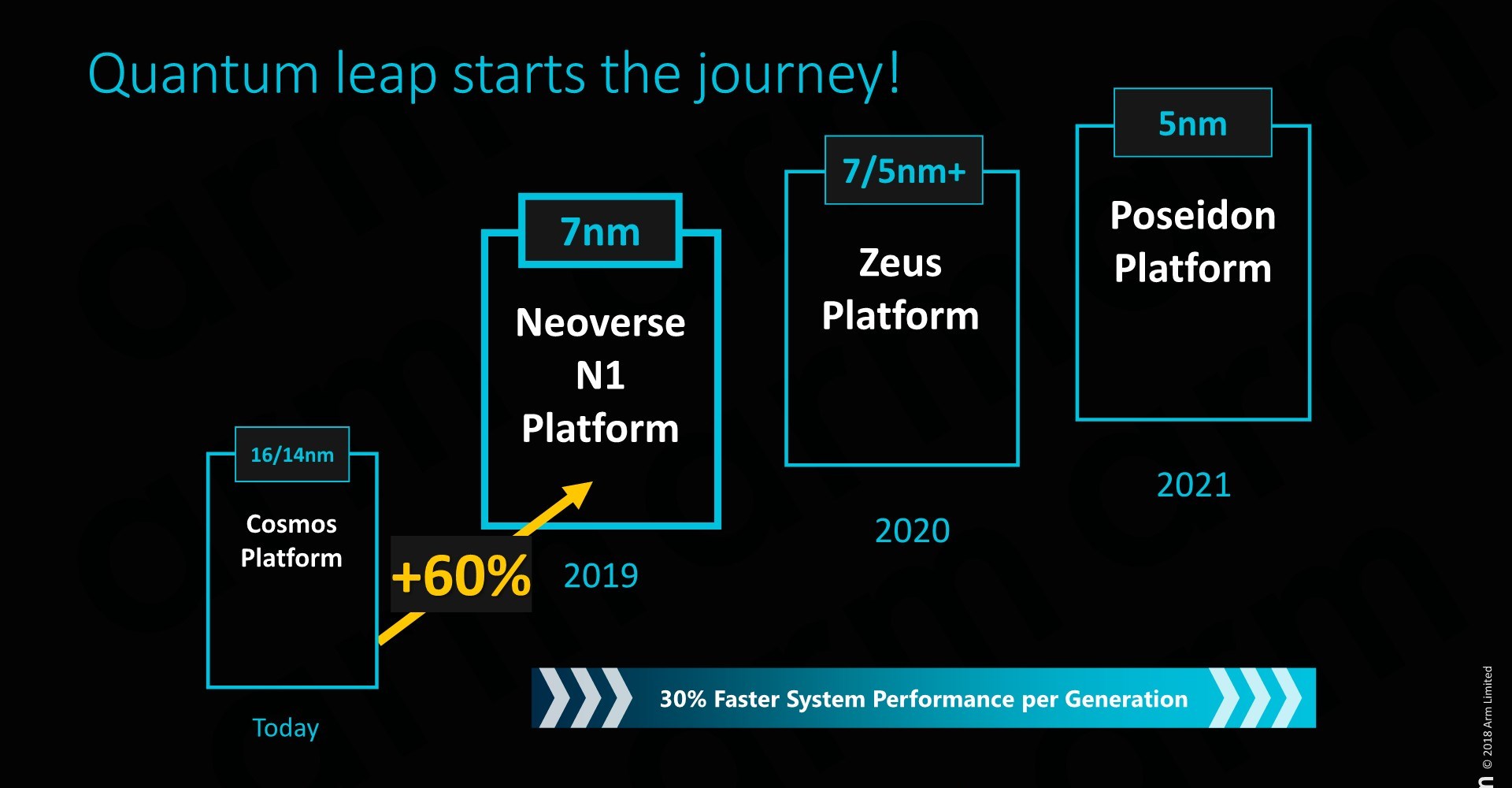
As mentioned in the introduction, the Neoverse N1 platform represents the first iteration of a new family of microarchitectures coming out of Arm’s Austin design centre. The N1, formerly known as “Ares”, represents the sever core counter-part to the “Enyo” Cortex-A76 µarch. The Austin team has likely already finished work on Zeus (consumer variant: Deimos) and we’re expecting Poseidon (consumer: Hercules) to be the final iteration of this family before the torch is passed on to the next microarchitecture family, likely currently being worked on by the Sophia-Antipolis design team.
The N1 CPU micro-architecture
With the N1 CPU being the infrastructure sibling of the Cortex-A76, it’s natural that we see a lot of similarities between the two cores. We’ve had the pleasure to cover the A76’s µarch disclosure last year in detail, and much of what we’ve covered in terms of the inner-workings of the new micro-architecture will also apply to the N1, with some notable differences that adapt the core for infrastructure use-cases.

In terms of high-level design goals, Arm’s target seems to be fairly straight-forward: Create a no-compromise microarchitecture that will be able to serve as the foundation that will be iterated on in the next several years.
In particular one design goal that also mirrors what we’ve seen in the Cortex A76 is that Arm is tailoring the microarchitecture to be able to run at maximum frequency in infrastructure deployments. This is in contrast to the strategy that AMD and Intel are employing for their server CPUs, where the products may have the same or similar microarchitectures to their consumer counter-parts, however come with much more limited clock frequencies. The advantage here for Arm is that this allows them to simultaneously optimise performance, power and area all at the same time, while Intel and AMD might have to compromise in one of these metrics depending what market segment is targeted with a given SKU.

The N1 CPU shares the same pipeline organisation we’ve seen on the Cortex A76. At the heart, this is a 4-wide fetch/decode machine with a very short pipeline depth of only 11 stages. Arm calls this an “accordion” pipeline because depending on the instruction, it’s able to reduce the length down to 9 stages in latency-sensitive situations. The second predict stage is able to overlap with the first fetch stage, and the dispatch stage is able to overlap with the first issue stage, same as on the A76.
The execution back-end also looks largely identical to the Cortex A76: We have 2 simple ALUs, one complex ALU which handles complex operations such multiplications and division, and two full-width 128b SIMD pipelines which handle vector as well as floating point operations.
Data throughput is an important aspect of the microarchitecture and here Arm again sees the deployment of two 128bit load/store units, able to sustain sufficient bandwidth to feed and service the execution pipelines.
The front-end of the CPU continues on sharing similarities with the Cortex A76: we’re seeing large L1 and L2 with low latency access. Arm here also employs some of the biggest branch target and direction prediction buffers that are publicly known in the industry, showcasing a big focus on trying to improving performance not just by having a wide core, but rather by trying to keep data flowing through the core by minimising both branch as well as cache misses.
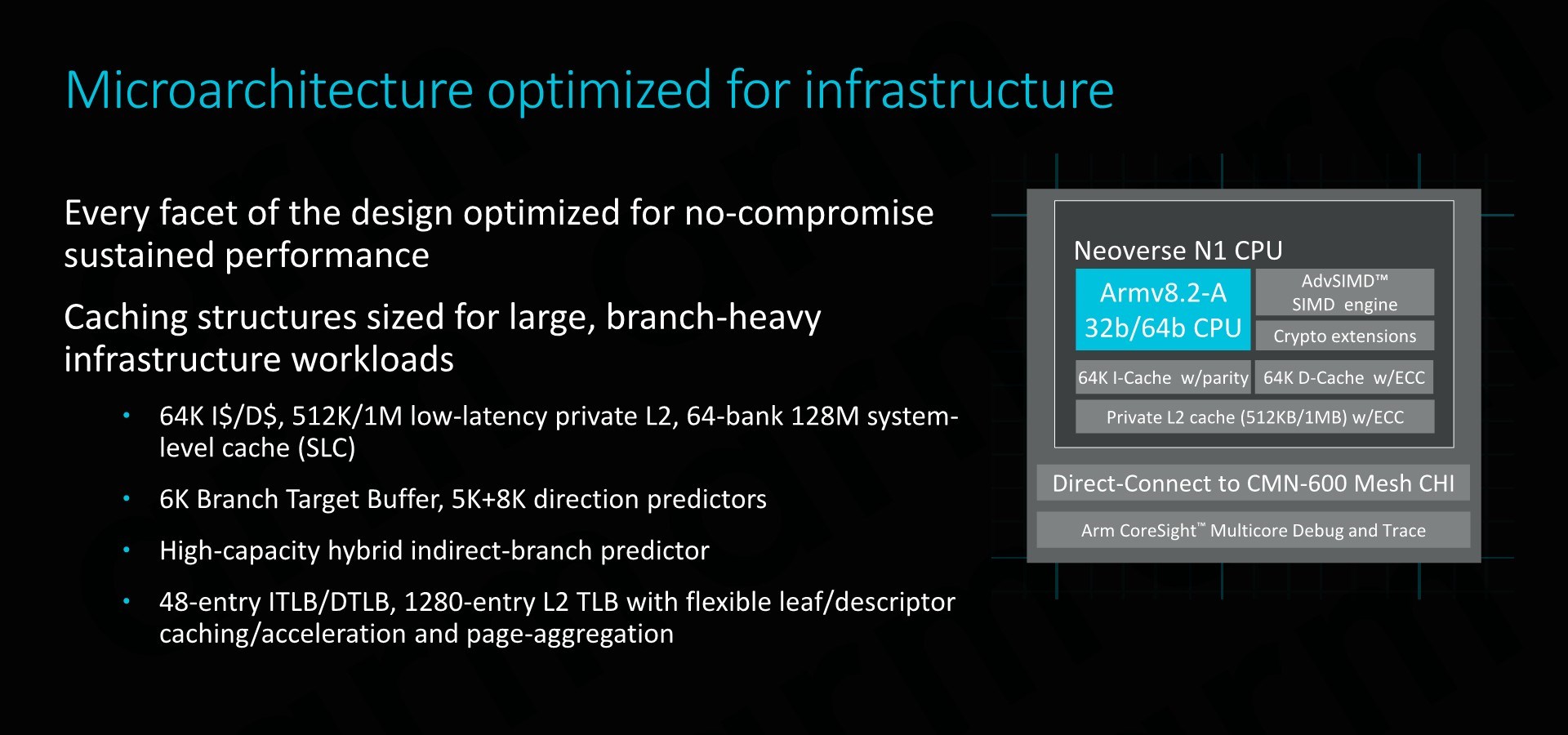

The cache hierarchy is one aspect where the N1 CPU differs more considerably from the A76. At the lowest level, the L1 cache still offers the same 64KB capacity with 4-cycle LD-use as its sibling, however the big important novelty on the N1 CPU is that now the cache is fully coherent. It’s noted that hardware I-cache coherency isn’t something that is required by the ISA and usually the way things have been done till now is through software maintenance operations. Getting hardware coherency implemented for the N1 was very important for Arm as it vastly improves performance and simplifies implementation of virtual environments, something that Arm needed to have if it wanted to be competitive among hyperscale customers. Having I-Cache coherency is noted to be a key enabler in order to scale the system for very large core-counts, and Arm describes it inherently a must-have for any system with a coherency plane of more than 16 cores.
The L2 cache is offered either in 512KB or 1MB options. The 512KB configuration matches what was available on the A76, while the addition of a 1MB cache likely targets heavier memory footprint applications in the infrastructure segment. It’s to be noted that doubling the L2 cache to 1MB doesn’t come without cost: the latency of the cache in this configuration sees a 2-cycle degradation, reaching a load-use latency of 11 cycles.
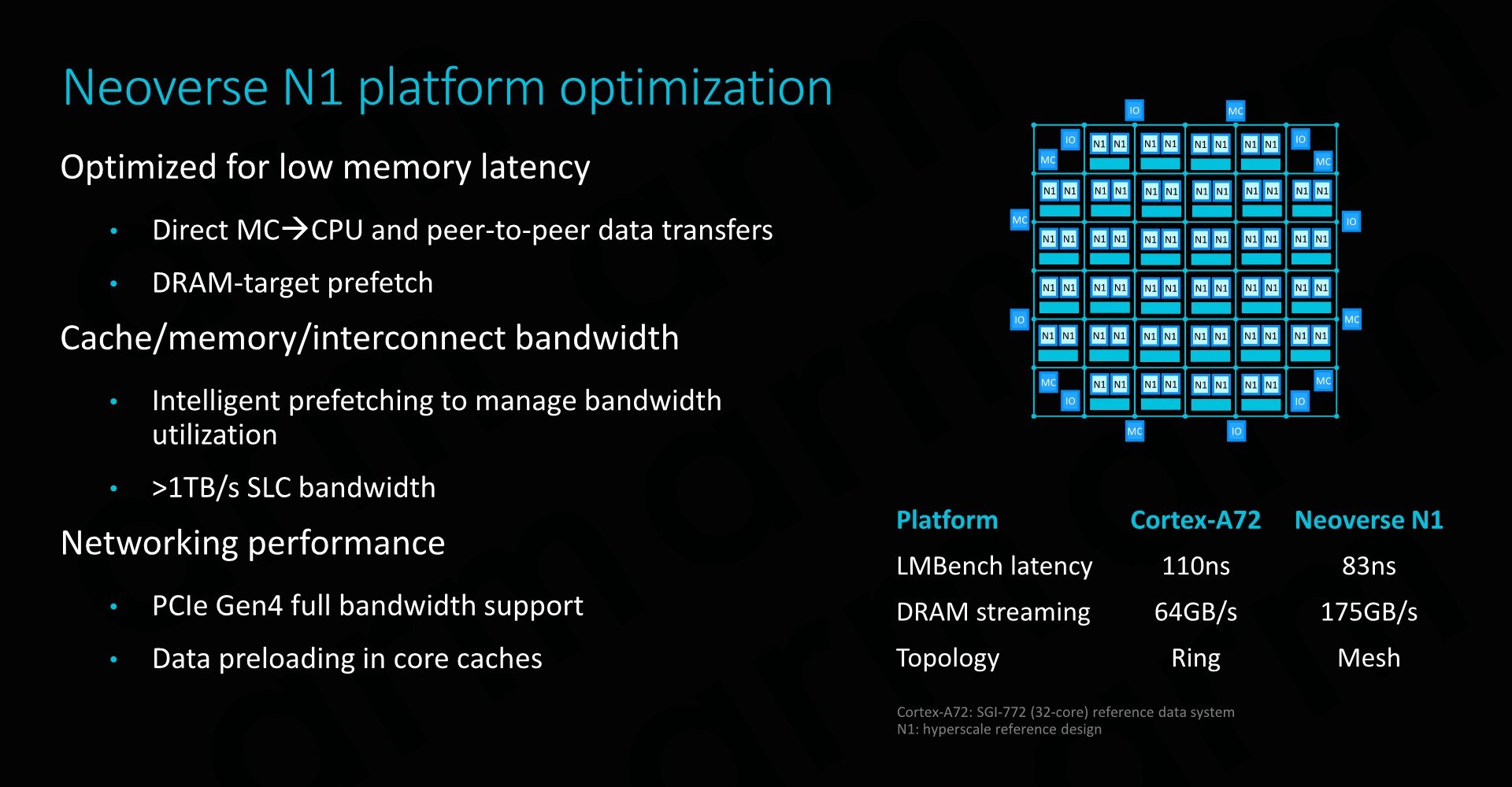
An immense difference to the Cortex A76 is when we go higher up the memory hierarchy. Instead of finding a cluster, the N1 CPU connects to a mesh interconnect. In particular we’re talking about Arm’s CMN-600 Coherent Mesh Network.
As depicted in the graph, this connection first follows through a CAL, or Component Aggregation Layer. Each CAL supports only up to two interfaces, which is why we only see two CPUs per “cluster” (it’s not really a cluster per se). The CAL then connects to an XP (Crosspoint) of the mesh, which essentially the switch/router component of the network. Each XP has two ports available; in the case of Arm reference design example the second port connects a SLC (System Level Cache) slice.
In an example configuration with 2MB SLC slices in a 64-core system (32 banks/slices), the average load-use latency for the whole 64MB cache would be 22ns. The reason that Arm gives the latency figures in ns rather than in cycles is because the SLC and mesh run on a different clock plane than the CPUs, usually at about 2/3rd the frequency of the cores.
Direct connect is an integral feature of the N1 and the CMN-600. This is a feature that only exists on this platform and something that isn’t possible on Cortex CPUs. Essentially it removes all the L3 and snoop-filter logic of the DSU and instead it directly connects the CPU cores to the CMN’s CHI’s interfaces. Thus essentially communication between the memory controller and the CPU core only has to pass through one intermediate layer, which is the mesh network itself. This might sound like something obvious coming from a traditional PC and server CPU background, but it’s an important distinction to make considering Arm’s history coming from mobile SoCs where data transfers have to go through cluster-level logic first.
Direct MC -> CPU data transfers might be a bit of confusing term to explain. Here when a CPU makes a data-request to the MC (Memory controller), it’s able to immediately and concurrently first send a “prefetch” type request directly to it, while at the same time the normal transfer command goes through the snoop-filter of the home-node of the XP in the mesh network, and then routing the request to the memory controller. Thus the MC will know in advance the request is coming and will have already started to get the data, hiding part of the effective memory latency than if the whole transfer would have happened in serial sequence.
Prefetching is extremely important to the performance of the whole system, and here data prefetching is intelligently managed to optimise system-level bandwidth.
In the example N1 reference system with 64 cores and 8 DDR-3200 memory channels, the N1 is said to achieve up to 175GB/s of DRAM streaming bandwidth. Arm also publishes latency numbers, but it’s to be noted that it’s a bit hard to make direct comparisons: Arm’s figures represent LMBench figures while configured with 2MB hugepages at a 256MB test depth. The choice of hugepages reduces TLB misses and gets nearer to the actual memory latency, and this was the rationale behind Arm publishing the metric under these circumstances.
We haven’t had the opportunity to test competing systems with hugepages enabled, but an AMD’s Epyc 7601 (LRDIMM DDR4-2666 19-19-19) will achieve ~73ns with an LMBench-like test at the end of the chip’s cache hierarchy, while a custom developed latency test minimising TLB misses to a minimum showcases a DRAM-load-use of around 57ns. An Intel W-3175X (RDIMM DDR-2666 24-19-19) system under the same tests achieved respectively 94ns and ~64ns. Again it’s hard to come to any hard conclusions here and the metrics aren’t directly comparable to Arm’s figures - we’d have to see a full latency curve of different tests to better determine things.
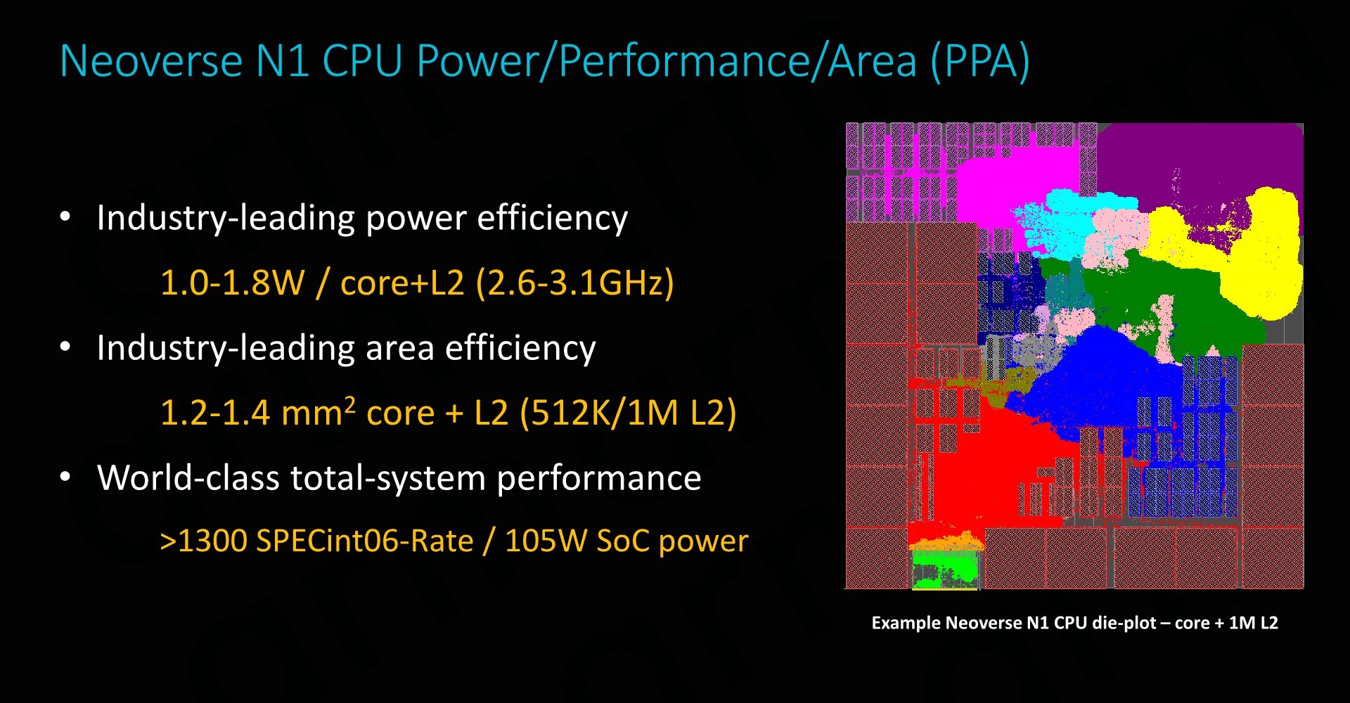
The N1 CPU when implemented on a 7nm TSMC process remains an extremely tiny piece of silicon. For an implementation with 512KB L2 cache Arm discloses a die size of 1.2mm², nearly identical the 1.26mm² footprint we measured a Cortex A76 on the Kirin 980. Doubling the L2 cache to 1MB raises the footprint by 0.2mm² to 1.4mm² per core.
In terms of frequency range, Arm envision 2.6GHz to 3.1GHz. The lower figure is quoted at a process nominal voltage of 0.75V while the 3.1GHz figure is under overdrive at 1V. It’s to be noted that the 19% higher frequency would come with a 44% higher power cost, so most vendors will want to stay nearer to the more efficient part of the power curve. In absolute figures, this is still only 1.0 to 1.8W. 1W gives plenty of headroom for a 64-core SoC while still remaining under some impressive total SoC power levels. Here Arm’s 64C N1 reference design would come at a total power budget of around 105W. We’ll be addressing the performance figures on the next page.


101 Comments
View All Comments
Santoval - Thursday, February 21, 2019 - link
"Both Intel and AMD have been making chips that take the CISC instructions and run them through an instruction decoder that then hands RISC instructions to the actual cpu."The instruction decoder is also part of an "actual CPU". Beside the decoder the front-end also has instruction fetch, a branch predictor, predecode (potentially), μOP & L1 instruction cache, instruction queues, a TLB, allocation queues etc etc All these units are most certainly parts of the "actual CPU".
I believe you rather meant "hands RISC-like instructions to the *back-end* of the CPU".
FunBunny2 - Thursday, February 21, 2019 - link
"The speed advantages on paper between RISC and CISC are in theory a wash. "not to keep beating the dead horse 360, dated as it is, but with the hardware of the time (and IBM was the top of the heap, then) the 360/30 ran the instruction set in micro-code. allegedly the first computer to even have microcode. ran like drek compared to the all-hardware versions of the machine. the '30 real cpu was long reputed to be some DEC machine.
"cpu design quite a bit without being so closely tied to backwards compatibility."
lots of folks say that, but makes no sense to me. compilers target the instruction set, which only changes when Intel publishes 'extensions'. whether those instructions are executed in pure ISA hardware, or a rat running in a spinning wheel (RISC), makes no difference to the compiler writer.
the profiling explanation for microcode over pure ISA hardware makes the most sense.
Wilco1 - Wednesday, February 20, 2019 - link
The only misinformation is from you. RTL simulation is widely used in the industry and is quite accurate.Studies have shown CISC instructions don't do more than RISC instructions - partly because compilers avoid CISC instructions, partly because CISC instructions are slow. That's why RISC works. But I wouldn't expect you to understand this.
FunBunny2 - Thursday, February 21, 2019 - link
"Studies have shown CISC instructions don't do more than RISC instructions "at least in the z world (and predecessors), there were/are some (I don't remember the count) of 'COBOL assist' instructions which were/are quite complex and were introduced to reduce the amount of times the COBOL coders had to 'drop down to assembler'. whether that's still true, I can't say.
DigitalVideoProcessor - Thursday, February 21, 2019 - link
CISC vs. RISC is a debate about instruction decode philosophy and it has almost zero bearing on the performance of a system. CISC machines reduce everything to RISC like operations. Saying one does more than another in a given clock is misinformation.melgross - Thursday, February 21, 2019 - link
Those wars are long over. No modern chip is either pure CISC or RISC. Those are long gone.Calin - Thursday, February 21, 2019 - link
SPECint, SPECfp, ... are "work done tasks" - what your're referring to was "MIPS" (or millions of instructions per second). This performance metric has lost its charm since internally x86 processors no longer use x86 instructions but large bundles of microoperations that are done in parallel and can be interleaved (so two instructions that follow each other are broken into micro operations which are reordered, and might be finalized in a different order).Kevin G - Thursday, February 21, 2019 - link
The thing is that real distinction of CISC vs. RISC is lost in their similar implementations: pipelined OoO parallel execution engines. While CISC encoding may* permit more operations to be contained within a single instruction but at the cost of having to decode that instruction into an optimal arrangement given the hardware. The price paid is in power consumption and complexity which may impact factors like maximum clock speed. In the era of many core and power limitations, these attributes are the foundation for RISC to have an edge over legacy CISC designs. Not to say that RISC architectures can't leverage instruction decoding either: expanding out the fields for registers to account for the larger rename register space is a simple procedure.Once chips begin parallel execution, the CISC advantage of doing more per instruction really starts to fall apart. The raw amount of work being done per cycle approaches the common limit of just how much parallelism can be extracted by an inherently serial stream of instructions. Arguably CISC designs can hit this sooner in terms of raw instruction count as the instruction stream is _effectively_ compressed compared to RISC.
*The concept of fused-multiply add instructions was an early staple of RISC architectures. Technically it goes against the purest ideal but traditional RISC designs permitted the number of operands in their instruction formatting to pull this off so they took advantage of an easy performance boost. x86 didn't gain this capability until AVX2 a few years ago.
peevee - Tuesday, February 26, 2019 - link
"I think you are forgetting the very nature of RISC (Arm) vs CISC (x86) architectures"This distinction does not exist in practice for decades.
wumpus - Wednesday, February 20, 2019 - link
It also shows a result showing Zen roughly half the performance of Intel, something that implies a fairly contrived situation. FX8350 might have had half (or worse) than Intel, but Zen is another story.I'm guessing that this involves AVX256 (or higher) specifically optimized for Intel (note that going to AVX512 is only a modest increase since the clockrate is brutally lowered to compensate for the increased power load. Also note that Zen2 (EPYC2 and Ryzen3000) will include native AVX256 execution paths).