Intel Process Technology Update: 10nm Server Products in 1H 2020, Accelerated 7nm in 2021
by Anton Shilov on May 8, 2019 3:29 PM EST- Posted in
- Semiconductors
- Intel
- 10nm
- EUV
- 7nm
- Manufacturing
Intel provided an update regarding its upcoming fabrication technologies at its 2019 Investor Meeting. The company is on track to produce server-class products using its 10 nm manufacturing technology already in the first half of 2020, which is something that the company implied on for a while now, but never confirmed officially. What is relatively surprising is that Intel intends to start production of ccommercial chips using its 7 nm process already in 2021.
Intel’s 7 nm production technology had been in development independently from the 10 nm process and by a different crew, so this one is closer than one might think. The node is set to use extreme ultraviolet lithography (EUVL) with laser wavelength of 13.5 nm for select layers, so it will not heavily rely on multipatterning, a major source of problems with Intel’s 10 nm process. In fact, the use of EUV will simplify development of products, make it easier to produce them, and will likely shorten production cycle times too.
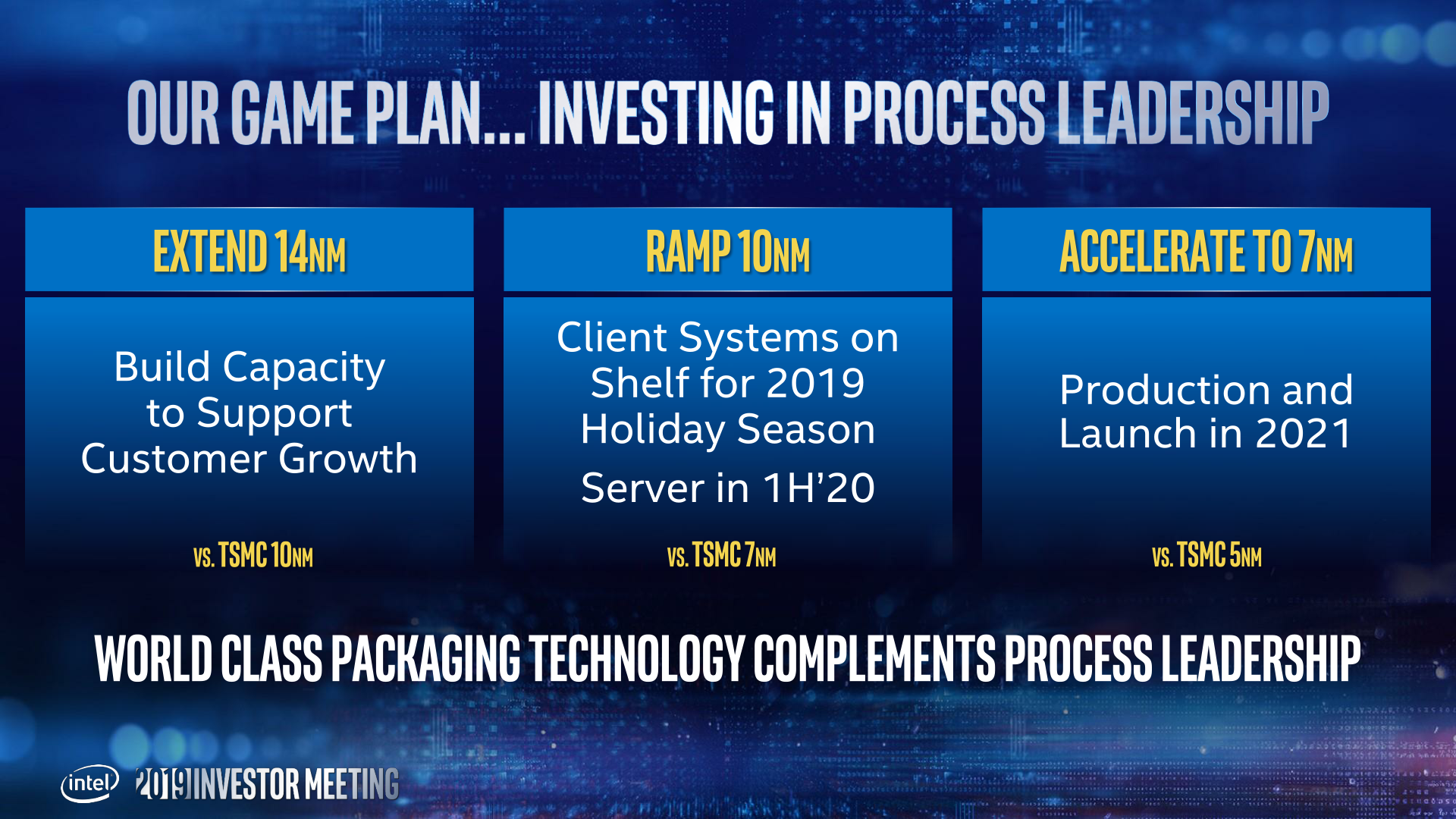
The first product to use Intel's 7 nm process technology will be Intel's Xe-architecture-based GP-GPU in 2021. The GPU will not only be made using Intel’s most advanced node, but will also us Intel’s Intel’s Embedded Die Interconnect Bridge (EMIB) technology as well as Foveros silicon stacking technique, which confirms that the product is not a monolithic design.
Speaking of non-monolithic designs, it is noteworthy that Intel considers its innovative chip packaging technologies no less important than its new nodes, so expect things like EMIB and Foveros to be a big part of Intel's future.
While Intel's first 7 nm product will be launched in 2021, Intel stresses that high-volume manufacturing (HVM) using the technology will begin in 2022 when the technology will be used not only for a server GPU, but also a server CPU. So, expect more 7 nm products three or four years down the road.

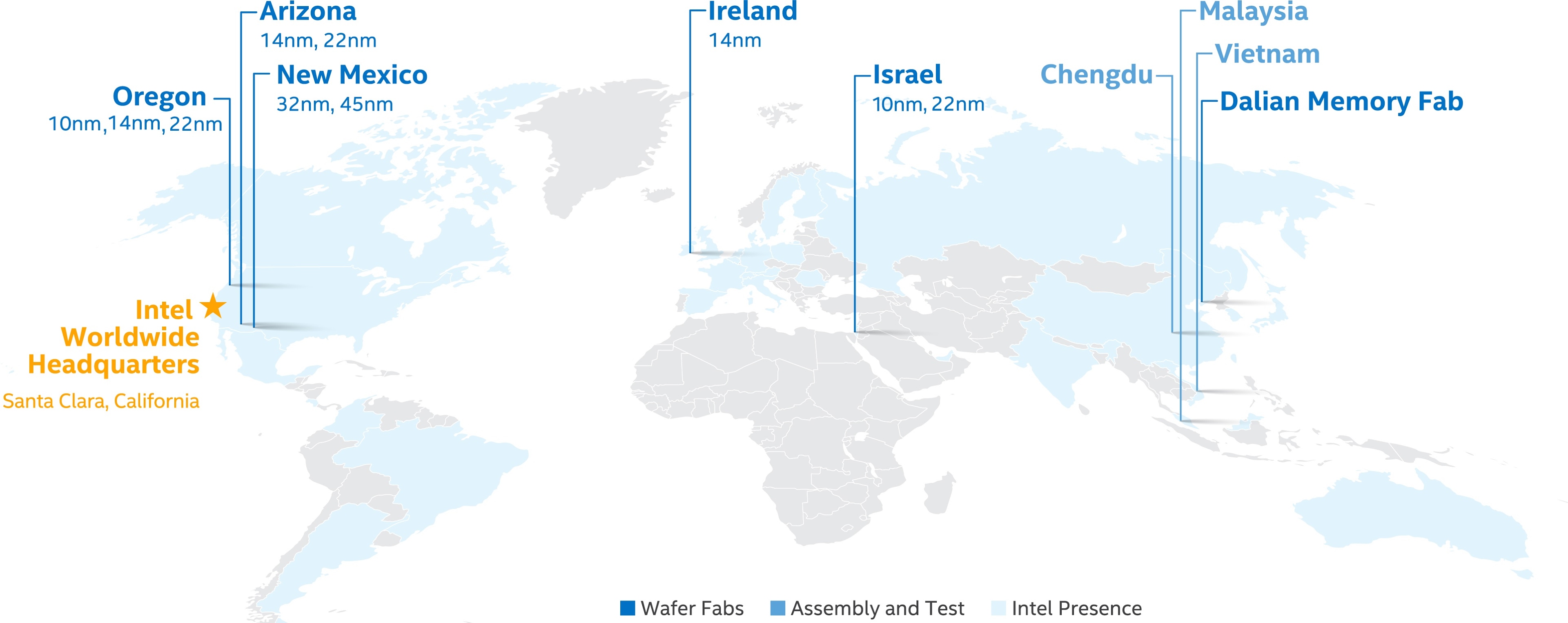
Late last year Intel announced a major plan to upgrade a number of its fabs for next-generation process technologies. Officially, Intel is equipping its Fab 42 in Arizona to make chips using its 7 nm fabrication process. Meanwhile, given the scope of Intel’s upgrade plan, which includes fabs in Oregon, Ireland, and Israel, it looks like the company might have other fabs ready for 7 nm by 2021 - 2022 timeframe.
Meanwhile, as Intel intends to refine all of its fabrication processes in the same manner as it did with its 14 nm node, expect Intel's 10 nm to co-exist with 7 nm for years.
Related Reading:
- Intel: EUV-Enabled 7nm Process Tech is on Track
- Intel Starts Qualification of Ice Lake CPUs, Raises 10nm Volume Expectation for 2019
- Intel Agilex: 10nm FPGAs with PCIe 5.0, DDR5, and CXL
- Intel to Equip Fab 42 for 7 nm
- Intel Discloses Plans to Spend $5 Billion on Fab 28 Expansion in Israel
- Intel Submits Ireland Fab Expansion Plan: $8 Billion Price Tag, With a 4 Year Lead Time
- Intel Details Plans for Its Oregon Fab Expansion: D1X Phase 3
- Intel to Expand Production Capacities at Multiple Fabs
Source: Intel


71 Comments
View All Comments
Marlin1975 - Wednesday, May 8, 2019 - link
But what type of "10nm" is this? Whats the density?Saying 10nm means nothing since they have changed designs to get a better yields.
Arsenica - Wednesday, May 8, 2019 - link
The last public details of Intel's 10nm (P1274) showed it was tied with TSMC's 7nm (7FF) in density metrics (54 nm as contacted gate pitch for both processes).As the slide still compares it to TSMC's 7FF is to be expected that their density is still comparable, but we'll only know for sure once somebody cleaves a shipping processor and measures it.
peevee - Thursday, May 9, 2019 - link
Newsflash: today Intel announced long-awaited release of a new code name. "Specious Lake represents the last 10 years of Intel innovation" said Super Vice President of Marketing Patel Dumborajachurpan.RSAUser - Tuesday, May 14, 2019 - link
Not sure where you heard that Intel 10nm is close to TSMC 7nm? Pretty sure that's wrong.Plus TSMC has stated that they are already offering 5nm in 2020, iPhone 2020 already confirmed that it's going to be using it.
bobhumplick - Wednesday, May 8, 2019 - link
you mean you think they have changed it. no one has any information confirming it. besides who cares. its just for mobile. the real piece of info here is 7nm. no more quad patterning. maybe no more dual patterning. better yields. faster chips. cant wait. my old 8700k will last me fine till then. was gonna get some really fast ddr4 but might just wait for ddr5 and 7nmSantoval - Wednesday, May 8, 2019 - link
Intel has long (*very* long) reported a transistor density of ~102 million transistors per mm^2 at 10nm. Intel's 7nm node was originally planned for a staggering 250+ MTr/mm^2 transistor density, but more recently -basically a bit after Brian Krzanich stepped down- I heard about densities in the order of ~200+ MTr/mm^2.Apparently Robert Swan set up a saner and more conservative target because he wants to avoid a repeat of the 10nm node fiasco, just like he should. Or he is listening to what his head engineers are saying is possible for 7nm, at least without blowing all their (publicly announced) deadlines and overshooting their allocated budget.
Santoval - Wednesday, May 8, 2019 - link
p.s. According to SemiWiki, to give you a comparison, TSMC at 7nm (non EUV) has a "minimum" transistor density of ~97 MTr/mm^2 but their 2nd gen 7nm node with EUV and their 6nm node will both have a 18% higher density of ~114 MTr/mm^2.Samsung will start at ~95 MTr/mm^2 and end up at 113 MTr/mm^2 in the third iteration of either their 7nm node or 5/6nm node (they say the node number is unclear).
So both Samsung and TSMC at 7nm are comparable to Intel at 10nm in terms of transistor density, but we do not yet really know how the high power variant of either of these nodes performs, or rather the sole such sample we have is Radeon VII. Intel released a sole 15W Core i3 with atrocious clocks (and a disabled iGPU) but that was the first unfixed iteration of their 10nm node. Ice Lake will sport the presumably fixed 10nm+ node. No data yet from Samsung's 7nm node.
FullmetalTitan - Thursday, May 9, 2019 - link
The kicker here is in the fine print. The Intel density numbers assume you are using high density libraries, when in fact their 10nm SDK has 3 different libraries of transistors. The high density cells are >100MT/mm^2, but the highest performance library is more like 60MT/mm^2 or less. I don't think TSMC or Samsung have released density figures with that granularity, but I assume all three are using similar marketing tactics to sound the best.Wilco1 - Thursday, May 9, 2019 - link
The issue is that unlike Intel, most TSMC chips actually do use the dense libraries. That includes servers, for example Centriq does 45 MT/mm^2 on 10nm. Mobile 10nm SoCs like Kirin 970 get 57 MT/mm^2, while Snapdragon 845 does 56, so they are only ~25% denser.So 10nm Intel servers should achieve 75 MT/mm^2. However I bet they won't even get 40 MT/mm^2 given 14nm density is around 16 MT/mm^2.
ZolaIII - Thursday, May 9, 2019 - link
Intel CPU should achieve 50MT/mm² (10 nm) or 65MT at best with 7nm while ARM is achieved 96MT already (Kirin) which goes up to 120MT with usage of UHD libs on same 7nm TSMC node, 170MT on 5 nm and around 200 MT on N5+ (UHD lib probably). Theoretical all the node's are physically the same (really nm) so achievable density is also the same but we seriously need a new gate structure. FinFET never whose good for many things to start with. Whosent good for analogue at all nor mixed circuit's for that matter which means not good for transceivers, MOSFET's cetera. It whose an Intel's child all together on the quest & design methodology to ensure peak higher possible clocks, two fins instead one. Does that sound familiar & then let's tie even more fets together (high performance lib) to ensure even better drain so that pore thing could hit even more MHz. The strategy whose wrong from beginning all together. FinFET brought a modest bump (200 MHz) over the planar in terms of what is industrialy considerd as sustainable leak for a complex structure as transistor but with an almost 2x power cost in a idle state it also enabled higher density of around 20~25% compared to planar in terms of possible miniaturisation but again with much higher both design and manufacturing costs. The AMD's (& IBM's also) idea originally with SOI whose much better one overlay but they didn't had enough money to push it to the end so didn't the Global foundries. It remains to be seen how good will Gate All Around be but FinFET really needs to die for many reasons.