Intel Process Technology Update: 10nm Server Products in 1H 2020, Accelerated 7nm in 2021
by Anton Shilov on May 8, 2019 3:29 PM EST- Posted in
- Semiconductors
- Intel
- 10nm
- EUV
- 7nm
- Manufacturing
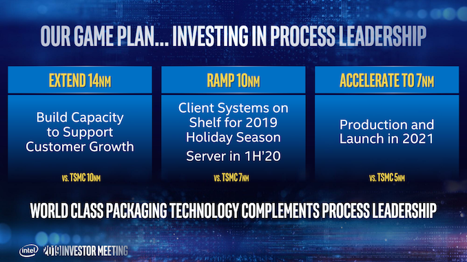
Intel provided an update regarding its upcoming fabrication technologies at its 2019 Investor Meeting. The company is on track to produce server-class products using its 10 nm manufacturing technology already in the first half of 2020, which is something that the company implied on for a while now, but never confirmed officially. What is relatively surprising is that Intel intends to start production of ccommercial chips using its 7 nm process already in 2021.
Intel’s 7 nm production technology had been in development independently from the 10 nm process and by a different crew, so this one is closer than one might think. The node is set to use extreme ultraviolet lithography (EUVL) with laser wavelength of 13.5 nm for select layers, so it will not heavily rely on multipatterning, a major source of problems with Intel’s 10 nm process. In fact, the use of EUV will simplify development of products, make it easier to produce them, and will likely shorten production cycle times too.
The first product to use Intel's 7 nm process technology will be Intel's Xe-architecture-based GP-GPU in 2021. The GPU will not only be made using Intel’s most advanced node, but will also us Intel’s Intel’s Embedded Die Interconnect Bridge (EMIB) technology as well as Foveros silicon stacking technique, which confirms that the product is not a monolithic design.
Speaking of non-monolithic designs, it is noteworthy that Intel considers its innovative chip packaging technologies no less important than its new nodes, so expect things like EMIB and Foveros to be a big part of Intel's future.
While Intel's first 7 nm product will be launched in 2021, Intel stresses that high-volume manufacturing (HVM) using the technology will begin in 2022 when the technology will be used not only for a server GPU, but also a server CPU. So, expect more 7 nm products three or four years down the road.
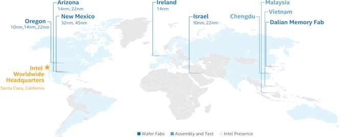
Late last year Intel announced a major plan to upgrade a number of its fabs for next-generation process technologies. Officially, Intel is equipping its Fab 42 in Arizona to make chips using its 7 nm fabrication process. Meanwhile, given the scope of Intel’s upgrade plan, which includes fabs in Oregon, Ireland, and Israel, it looks like the company might have other fabs ready for 7 nm by 2021 - 2022 timeframe.
Meanwhile, as Intel intends to refine all of its fabrication processes in the same manner as it did with its 14 nm node, expect Intel's 10 nm to co-exist with 7 nm for years.
Related Reading:
- Intel: EUV-Enabled 7nm Process Tech is on Track
- Intel Starts Qualification of Ice Lake CPUs, Raises 10nm Volume Expectation for 2019
- Intel Agilex: 10nm FPGAs with PCIe 5.0, DDR5, and CXL
- Intel to Equip Fab 42 for 7 nm
- Intel Discloses Plans to Spend $5 Billion on Fab 28 Expansion in Israel
- Intel Submits Ireland Fab Expansion Plan: $8 Billion Price Tag, With a 4 Year Lead Time
- Intel Details Plans for Its Oregon Fab Expansion: D1X Phase 3
- Intel to Expand Production Capacities at Multiple Fabs
Source: Intel


71 Comments
View All Comments
ZolaIII - Thursday, May 9, 2019 - link
The base DUV 7 nm TSMC is a very good base for calculation as it uses basic rooting lib. The HP lib basically ties more fin's per gate to ensure better connectivity & better drain so it's fair to split HP in half to get the base gate calculation. Intel doesn't give (nor use) base, HD or UHD libs only HP one to ensure brute forced higher clocks & it sips power like hell leaking all around.ajc9988 - Sunday, May 26, 2019 - link
TSMC has. Here are the two things you are looking for:https://fuse.wikichip.org/news/2004/iedm-2018-inte...
https://www.techcenturion.com/7nm-10nm-14nm-fabric...
Then, you should compare that to achieved densities like here:
https://www.anandtech.com/show/13687/qualcomm-snap...
0ldman79 - Friday, May 10, 2019 - link
Density is only part of the equation.Eventually there will be gaps in between the circuits and transistors as the gap will be too small for a dielectric to stop electromigration.
The density doesn't set the size of the transistors, it is just one side effect of the smaller lithography.
DanNeely - Wednesday, May 8, 2019 - link
I'll believe it when I can buy it.Coincidentally, 2021/22 is about when I'm due for a new desktop build; so I really am hoping Intel gets its stuff together and Intel and AMD are able to vigorously compete for my CPU dollars.
HStewart - Wednesday, May 8, 2019 - link
10nm desktop sounds like 1st half 2020 not 2021, this means less than year away since shortly it be starting 2nd half. and what does 1st half mean - any time between Jan and July 1.Wilco1 - Wednesday, May 8, 2019 - link
Do you seriously believe there will be 10nm 5GHz desktop chips next year?HStewart - Wednesday, May 8, 2019 - link
Desktop is now a minor market, but server will have new cpus's but with new architexture 5Ghz may not be necessary on Sunny Cove.Wilco1 - Wednesday, May 8, 2019 - link
Right, so you agree 10nm will never reach 5GHz?HStewart - Wednesday, May 8, 2019 - link
I did not say that - I say it may not have to - that is different. 5Ghz on current Intel architexture - may be slower than 3Ghz on Sunny Cove. If ALU's on CPU handle twice the instructions per clock cycle as previous architexture than 5 Ghz is not required.name99 - Wednesday, May 8, 2019 - link
Not if this is anything close to reality!https://browser.geekbench.com/v4/cpu/compare/11493...
https://browser.geekbench.com/v4/cpu/compare/13056...
Is is trustworthy (supposed to be an IL 1.4GHz base, 2.3GHz turbo)? Who knows, but it's better done than most fakes. Reveals an IPC very close to current i5 except for AES.