Intel Details Manufacturing through 2023: 7nm, 7+, 7++, with Next Gen Packaging
by Ian Cutress & Anton Shilov on May 8, 2019 4:35 PM EST
At Intel's Investor Day today, CEO Bob Swan and Murthy Renduchintala spoke to the ability of the company with respect to its manufacturing capabilities. Intel has historically been strong in its ability to execute on its process technology, however the delay of its 10nm process has obviously raised multiple question marks, and has done for several years. The two Intel executives went into a little detail about what Intel was doing in the interim, and how it has learned from the issues.
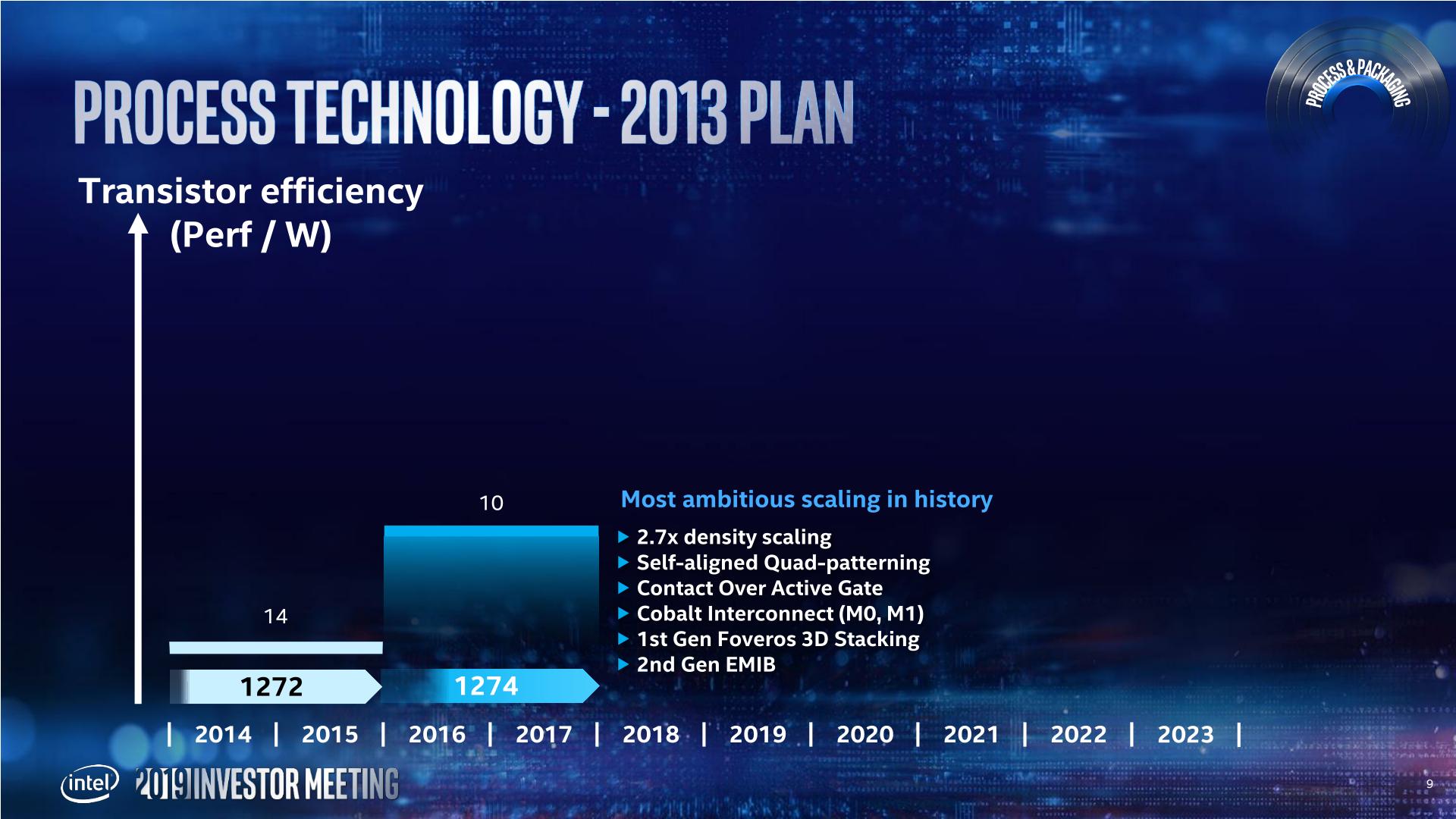
Back in 2013, Intel envisoned its 10nm to succeed the 14nm by providing 2.7x density, with new technologies such as Self-Aligned Quad Patterning (SAQP), Contact over Active Gate (COAG), Cobolt Interconnects, and new packaging technologies such as EMIB and Foveros. Intel admits that this was an ambitious plan, and the goals were not clearly defined with the teams and it was ultimately overly complex and not managed in an ideal way.
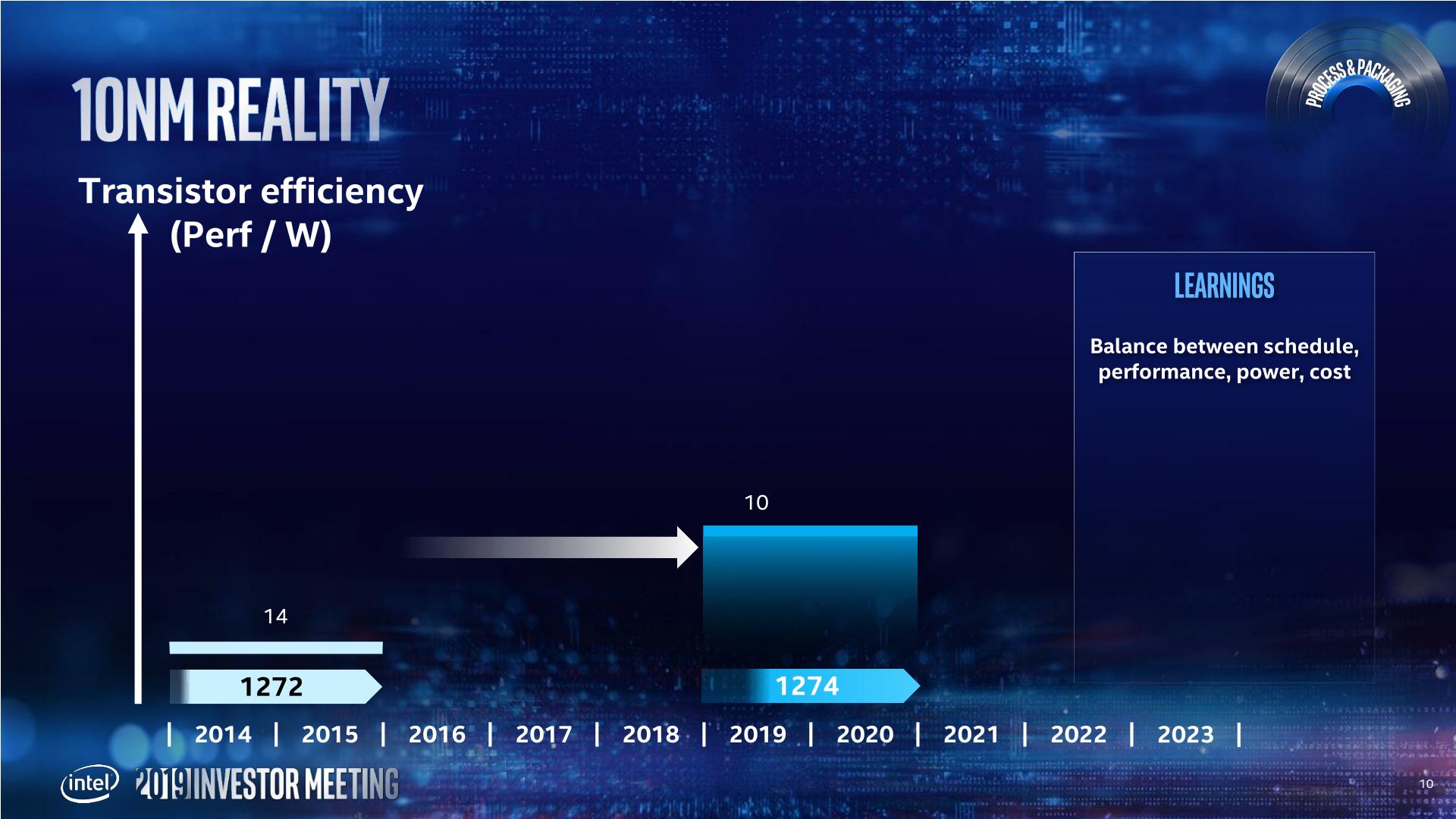
This ended up pushing 10nm out into a later time frame. In this case, Intel pushed 10nm out to 2019 (technically they shipped Cannon Lake in small quantities on 10nm in 2017, however that is nothing more than a curio in the timeline of semiconductors), and filled the gap with 14+ and 14++.
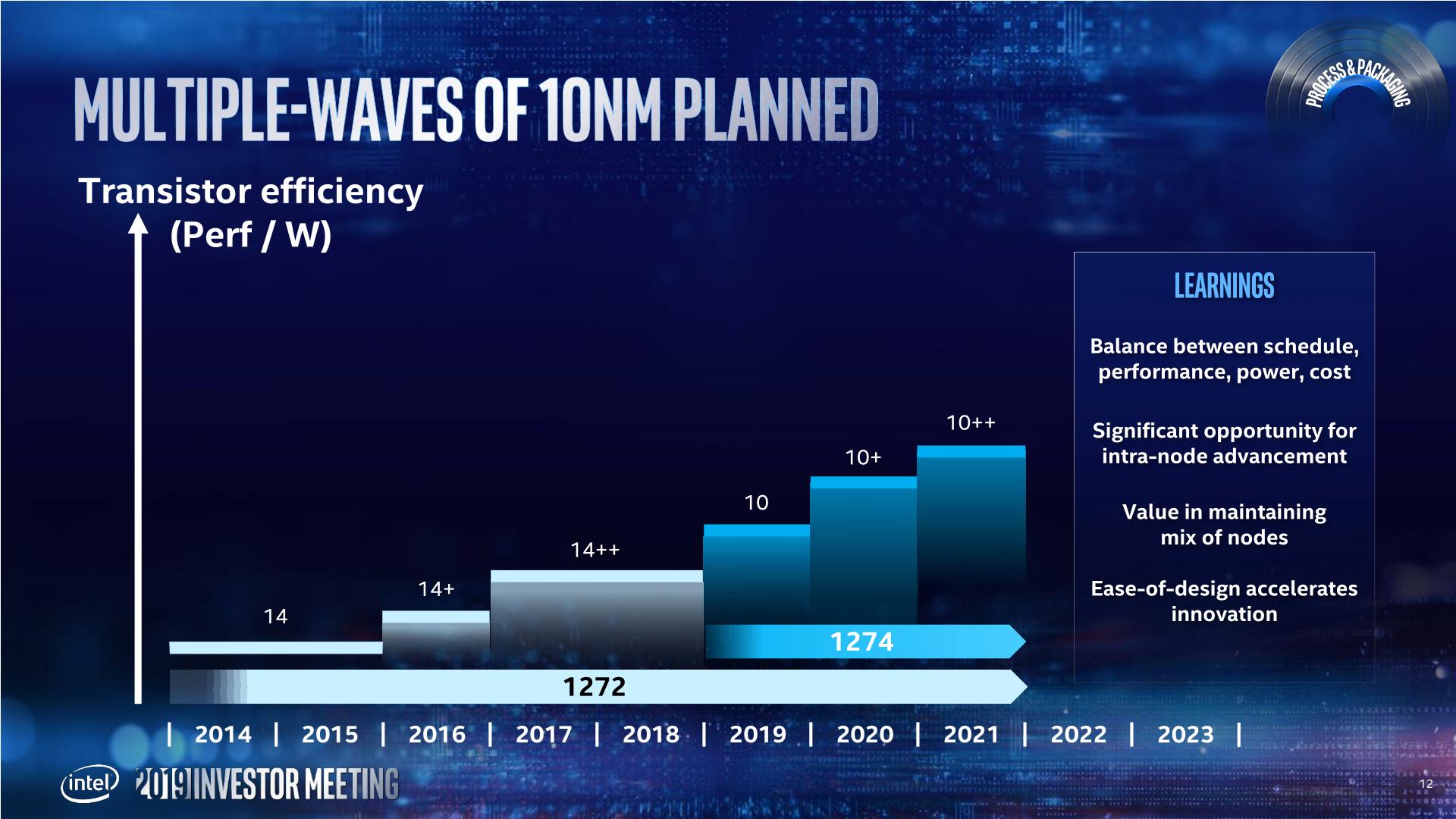
Intels 14+ and 14++ processes extracted more than 20% more performance (from Broadwell to Whiskey Lake) from the process since its inception. As a result, Intel is prepared to not only get ready for future intra-node optimizations, but actually adjust the roadmap to compensate for it. Murthy made it clear that Intel wants to introduce a Moore's Law-like gain at the beginning of a new process, and another similar gain by the end of the process.
Intel has stated that its 10nm product family (beyond Cannon Lake) will start to be available from the middle of this year (2019), with Ice Lake on client platforms (notebooks).

Intel will be launching multiple 10nm products through 2019 and 2020, including server based 10nm in the first half of 2020:
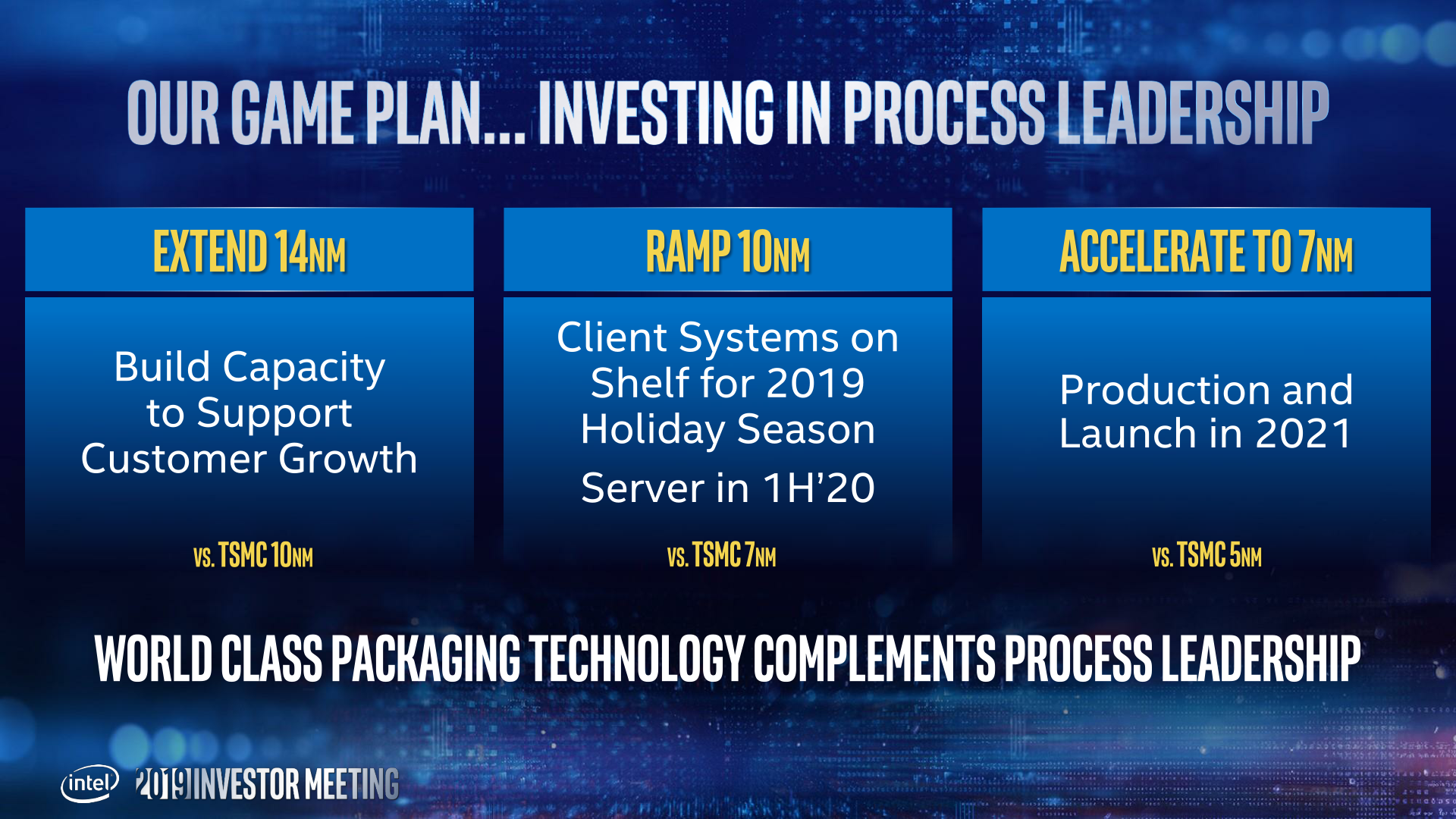
In the above slide, Intel states that it will have 7nm in production and launching a product in 2021. That sounds very aggressive for a company that has had issues with 10nm. It even shows in Intels radmap, with 10nm (and 10+ and 10++) having a much shorter life cycle than the 14nm family of processes.
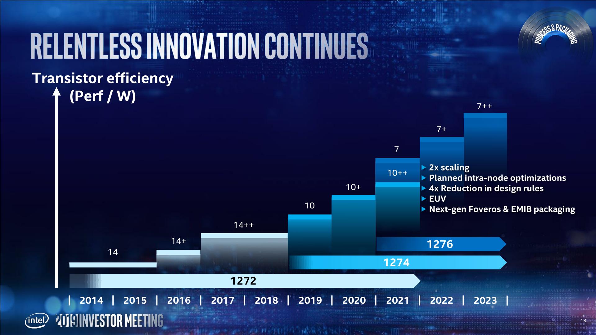
With this in mind, Intel's 7nm is going to be the combination of what Intel has learned from the 14nm and 10nm family of products. Intel wants that 2x scaling (Moores Law), but with intra-node optimations planned as part of the roadmap. Intel is also reducing its number of design rules, which should help with execution. 7nm will also be where Intel intersects with EUV, and also introduce next-gen Foveros and EMIB packainging.
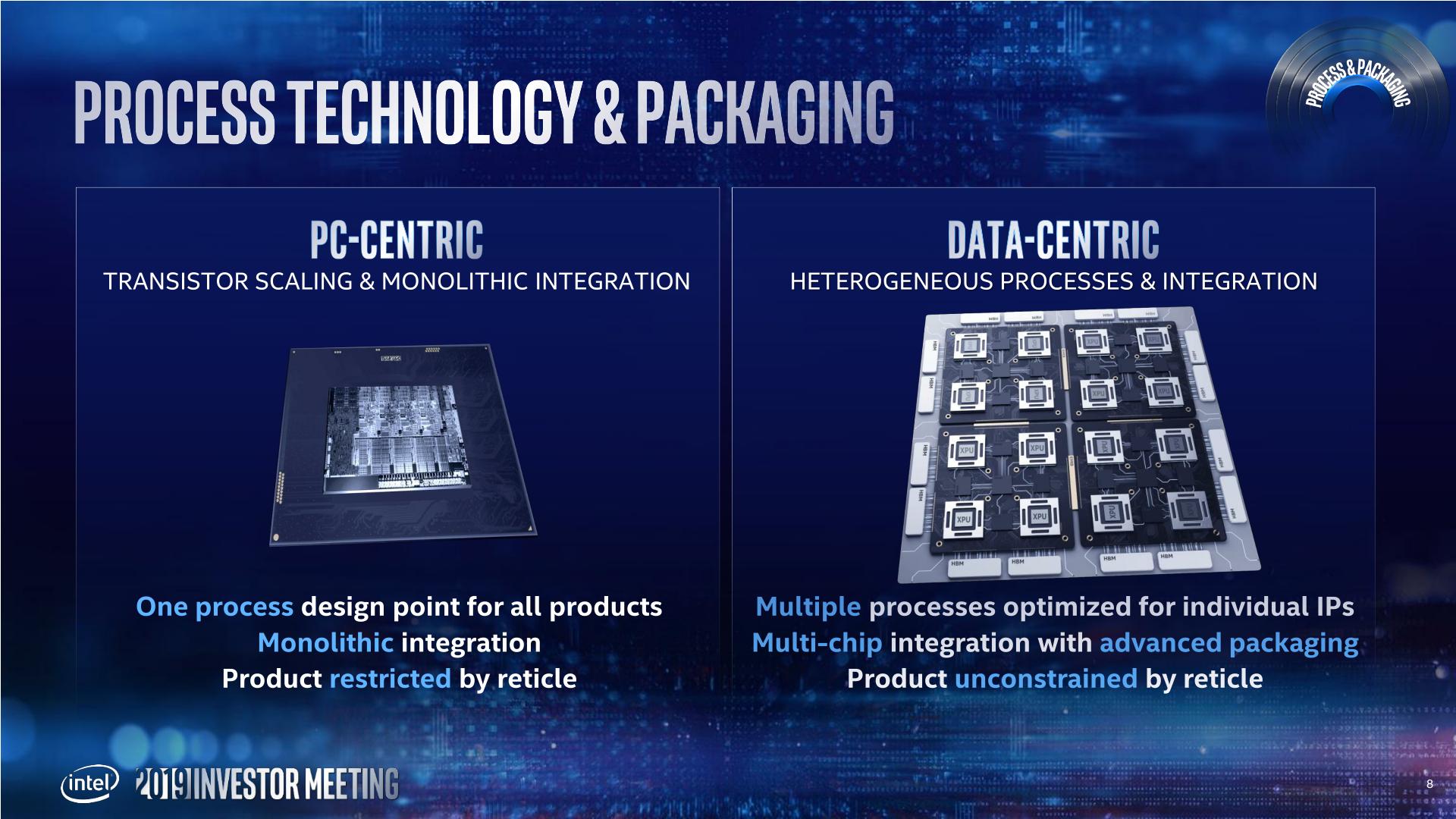
Intel provided this slide, which shows a monolithic PC-Centric die with a multi-die Data-Centric chip built on both Foveros and EMIB. This corroborates our discussion with Intel's chiplet and packaging team, who also stated that we would see Foveros and EMIB on a combined product - specifically the GPU.

Intel announced that its lead 7nm product (lead = top, or lead = first?) would be its new GPGPU, built on the Xe graphics architecture. Intel has stated that its Xe product stack will feature two different microarchitectures from mobile client up to GPGPU, with one of those architectures called Arctic Sound - technically Intel will launch its first discrete GPU in 2020 according to its press release, however the 7nm GPGPU will be launched in 2021.
More information is coming out of Intel's Event, more to follow.
Related Reading
- Intel: EUV-Enabled 7nm Process Tech is on Track
- Intel Starts Qualification of Ice Lake CPUs, Raises 10nm Volume Expectation for 2019
- Intel Agilex: 10nm FPGAs with PCIe 5.0, DDR5, and CXL
- Intel to Equip Fab 42 for 7 nm
- Intel Discloses Plans to Spend $5 Billion on Fab 28 Expansion in Israel
- Intel Submits Ireland Fab Expansion Plan: $8 Billion Price Tag, With a 4 Year Lead Time
- Intel Details Plans for Its Oregon Fab Expansion: D1X Phase 3
- Intel to Expand Production Capacities at Multiple Fabs
Source: Intel


237 Comments
View All Comments
HStewart - Thursday, May 9, 2019 - link
My guess high performance new architexture mobile system that also has long battery life. i7 quad core and likely higher. Plus a new breed of lake field device - extreme portability, long battery life and single core speed that high instead of slow.Keep in mind process is not everything, I believe the big surprise will be Sunny Cove which also means all HW Migrations done also. Not to mention integrated Gen 11 graphics at NVidia 1030 speeds
HStewart - Thursday, May 9, 2019 - link
Desktop supposedly comes to 6 months later which lines up to beginning on 2020, but who knows Intel may have yet another surprise in the works.Xyler94 - Friday, May 10, 2019 - link
So you're guessing on what exactly? Last time Intel "released" 10nm, it was on a super low powered chip on a single laptop meant for China. I really don't share your same enthusiasm over Sunny Cove. Because of the Haswell to Skylake era. Skylake was not that huge of an improvement over Haswell, even though it promised it was. Sure it was more efficient and overclocked a bit better, but in terms of gaming, it didn't help much more.Sunny Cove cores will be like Skylake cores, a small improvement. I don't expect great things from it... But I'd love to be proven wrong.
arashi - Saturday, May 11, 2019 - link
Based off his 30 years in Intel marketing.aryonoco - Thursday, May 9, 2019 - link
So, ignoring the nonsensical nm numbers by everyone, based on their own admission Intel is at least 2 years behind TSMC in using EUV?This is crazy. When FinFETs came around, Intel had a solid 2-3 year head start over everyone else in the industry. Now they are 2-3 years behind? What happened?!
This really is worse than the NetBurst debacle, and it's also much more costly and time consuming to rectify.
edzieba - Thursday, May 9, 2019 - link
"Now they are 2-3 years behind? What happened?!"Same as EUV for the past decade: cost continues to increase to implement, DUV continues to provide more value for the same output (i.e. every year EUV is pushed back is a year of SAQP improvements). Samsung, TSMC, and GloFo (until they dropped out entirely) have all progressively pushed back EUV implementation again and again, and even TSMC have stepped back from all-EUV to "we'll do it in at least one layer I guess" for a future process.
HStewart - Thursday, May 9, 2019 - link
Nothing like Netburst, except possibly saying what is coming next which is Sunny Cove in June.Nimrael - Thursday, May 9, 2019 - link
First of all, Zen2 will NOT use any of EUV processes. Only 193nm DUV CLN7FF.Even 13/5 EUV CLN7FF+ use only 4(four) of 14 layers in EUV. CLN6FF - up to 5 of 14.
Intel's 10nm DUV process approximately equal to the Zen 2's CLN7FF
peevee - Thursday, May 9, 2019 - link
"This really is worse than the NetBurst debacle"Not much of a debacle, P4 sold better than Athlons, and 4GHz 15 years ago was very impressive. On 90nm no less. Still ~real nm back then.
YoloPascual - Thursday, May 9, 2019 - link
You said in 2012 that we will have 10nm on 2015. Not gonna believe you anymore.