PCI Express Bandwidth to Be Doubled Again: PCIe 6.0 Announced, Spec to Land in 2021
by Ryan Smith on June 18, 2019 5:00 PM EST
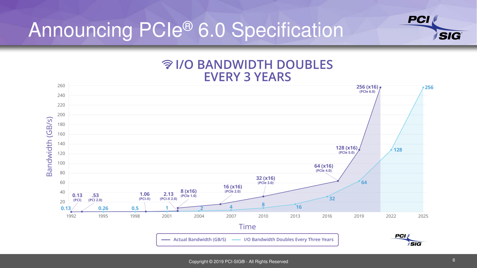
When the PCI Special Interest Group (PCI-SIG) first announced PCIe 4.0 a few years back, the group made it clear that they were not just going to make up for lost time after PCIe 3.0, but that they were going to accelerate their development schedule to beat their old cadence. Since then the group has launched the final versions of the 4.0 and 5.0 specifications, and now with 5.0 only weeks old, the group is announcing today that they are already hard at work on the next version of the PCIe specification, PCIe 6.0. True to PCIe development iteration, the forthcoming standard will once again double the bandwidth of a PCIe slot – a x16 slot will now be able to hit a staggering 128GB/sec – with the group expecting to finalize the standard in 2021.
As with the PCIe iterations before it, the impetus for PCIe 6.0 is simple: hardware vendors are always in need of more bandwidth, and the PCI-SIG is looking to stay ahead of the curve by providing timely increases in bandwidth. Furthermore in the last few years their efforts have taken on an increased level of importance as well, as other major interconnect standards are building off of PCIe. CCIX, Intel’s CXL, and other interfaces have all extended PCIe, and will in turn benefit from PCIe improvements. So PCIe speed boosts serve as the core of building ever-faster (and more interconnected) systems.
PCIe 6.0, in turn, is easily the most important/most disruptive update to the PCIe standard since PCIe 3.0 almost a decade ago. To be sure, PCIe 6.0 remains backwards compatible with the 5 versions that have preceded it, and PCIe slots aren’t going anywhere. But with PCIe 4.0 & 5.0 already resulting in very tight signal requirements that have resulted in ever shorter trace length limits, simply doubling the transfer rate yet again isn’t necessarily the best way to go. Instead, the PCI-SIG is going to upend the signaling technology entirely, moving from the Non-Return-to-Zero (NRZ) tech used since the beginning, and to Pulse-Amplitude Modulation 4 (PAM4).
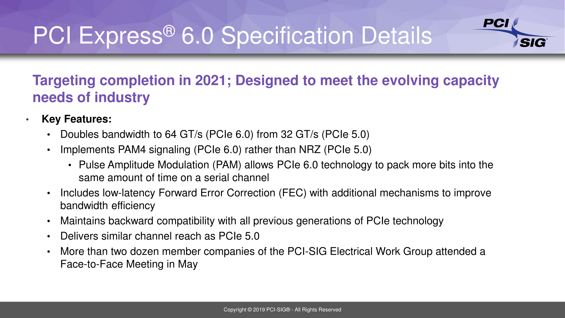
At a very high level, what PAM4 does versus NRZ is to take a page from the MLC NAND playbook, and double the number of electrical states a single cell (or in this case, transmission) will hold. Rather than traditional 0/1 high/low signaling, PAM4 uses 4 signal levels, so that a signal can encode for four possible two-bit patterns: 00/01/10/11. This allows PAM4 to carry twice as much data as NRZ without having to double the transmission bandwidth, which for PCIe 6.0 would have resulted in a frequency around 30GHz(!).
NRZ vs. PAM4 (Base Diagram Courtesy Intel)
PAM4 itself is not a new technology, but up until now it’s been the domain of ultra-high-end networking standards like 200G Ethernet, where the amount of space available for more physical channels is even more limited. As a result, the industry already has a few years of experience working with the signaling standard, and with their own bandwidth needs continuing to grow, the PCI-SIG has decided to bring it inside the chassis by basing the next generation of PCIe upon it.
The tradeoff for using PAM4 is of course cost. Even with its greater bandwidth per Hz, PAM4 currently costs more to implement at pretty much every level, from the PHY to the physical layer. Which is why it hasn’t taken the world by storm, and why NRZ continues to be used elsewhere. The sheer mass deployment scale of PCIe will of course help a lot here – economies of scale still count for a lot – but it will be interesting to see where things stand in a few years once PCIe 6.0 is in the middle of ramping up.
Meanwhile, not unlike the MLC NAND in my earlier analogy, because of the additional signal states a PAM4 signal itself is more fragile than a NRZ signal. And this means that along with PAM4, for the first time in PCIe’s history the standard is also getting Forward Error Correction (FEC). Living up to its name, Forward Error Correction is a means of correcting signal errors in a link by supplying a constant stream of error correction data, and it’s already commonly used in situations where data integrity is critical and there’s no time for a retransmission (such as DisplayPort 1.4 w/DSC). While FEC hasn’t been necessary for PCIe until now, PAM4’s fragility is going to change that. The inclusion of FEC shouldn’t make a noticeable difference to end-users, but for the PCI-SIG it’s another design requirement to contend with. In particular, the group needs to make sure that their FEC implementation is low-latency while still being appropriately robust, as PCIe users won’t want a significant increase in PCIe’s latency.
The upshot of the switch to PAM4 then is that by increasing the amount of data transmitted without increasing the frequency, the signal loss requirements won’t go up. PCIe 6.0 will have the same 36dB loss as PCIe 5.0, meaning that while trace lengths aren’t officially defined by the standard, a PCIe 6.0 link should be able to reach just as far as a PCIe 5.0 link. Which, coming from PCIe 5.0, is no doubt a relief to vendors and engineers alike.
Even with these changes, however, as previously mentioned PCIe 6.0 is fully backwards compatible with earlier standards, and this will go for both hosts and peripherals. This means that to a certain extent, hardware designers are essentially going to be implementing PCIe twice: once for NRZ, and again for PAM4. This will be handled at the PHY level, and while it’s not a true doubling of logic (what is NRZ but PAM4 with half as many signal levels?), it does mean that backwards compatibility is a bit more work this time around. Though discussing the matter in today’s press conference, it doesn’t sound like the PCI-SIG is terribly concerned about the challenges there, as PHY designers have proven quite capable (e.g. Ethernet).
| PCI Express Bandwidth (Full Duplex) |
||||||||
| Slot Width | PCIe 1.0 (2003) |
PCIe 2.0 (2007) |
PCIe 3.0 (2010) |
PCIe 4.0 (2017) |
PCIe 5.0 (2019) |
PCIe 6.0 (2021) |
||
| x1 | 0.25GB/sec | 0.5GB/sec | ~1GB/sec | ~2GB/sec | ~4GB/sec | ~8GB/sec | ||
| x2 | 0.5GB/sec | 1GB/sec | ~2GB/sec | ~4GB/sec | ~8GB/sec | ~16GB/sec | ||
| x4 | 1GB/sec | 2GB/sec | ~4GB/sec | ~8GB/sec | ~16GB/sec | ~32GB/sec | ||
| x8 | 2GB/sec | 4GB/sec | ~8GB/sec | ~16GB/sec | ~32GB/sec | ~64GB/sec | ||
| x16 | 4GB/sec | 8GB/sec | ~16GB/sec | ~32GB/sec | ~64GB/sec | ~128GB/sec | ||
Putting all of this in practical terms then, PCIe 6.0 will be able to reach anywhere between ~8GB/sec for a x1 slot up to ~128GB/sec for a x16 slot (e.g. accelerator/video card). For comparison’s sake, 8GB/sec is as much bandwidth as a PCIe 2.0 x16 slot, so over the last decade and a half, the number of lanes required to deliver that kind of bandwidth has been cut to 1/16th the original amount.
Overall, the PCI-SIG has set a rather aggressive schedule for this standard: the group has already been working on it, and would like to finalize the standard in 2021, two years from now. This would mean that the PCI-SIG will have improved PCIe’s bandwidth by eight-fold in a five-year period, going from PCIe 3.0 and its 8 GT/sec rate in 2016 to 4.0 and 16 GT/sec in 2017, 5.0 and 32 GT/sec in 2019, and finally 6.0 and 64 GT/sec in 2021. Which would be roughly half the time it has taken to get a similar increase going from PCIe 1.0 to 4.0.
As for end users and general availability of PCIe 6.0 products, while the PCI-SIG officially defers to the hardware vendors here, the launch cycles of PCIe 4.0 and 5.0 have been very similar, so PCIe 6.0 will likely follow in those same footsteps. 4.0, which was finalized in 2017, is just now showing up in mass market hardware in 2019, and meanwhile Intel has already committed to PCIe 5.0-capable CPUs in 2021. So we may see PCIe 6.0 hardware as soon as 2023, assuming development stays on track and hardware vendors move just as quickly to implement it as they have on earlier standards. Though for client/consumer use, it bears pointing out that with the rapid development pace for PCIe – and the higher costs that PAM4 will incur – just because the PCI-SIG develops 6.0 it doesn't mean it will show up in client decides any time soon; economics and bandwidth needs will drive that decision.
Speaking of which, as part of today’s press conference the group also gave a quick update on PCIe compliance testing and hardware rollouts. PCIe 4.0 compliance testing will finally kick off in August of this year, which should further accelerate 4.0 adoption and hardware support. Meanwhile PCIe 5.0 compliance testing is still under development, and like 4.0, once 5.0 compliance testing becomes available it should open the flood gates to much faster adoption there as well.


Source: PCI-SIG


119 Comments
View All Comments
Targon - Thursday, June 20, 2019 - link
The PC market became boring since the second generation Core i series of chips, and people saw little reason to upgrade their computers, including enthusiasts. With AMD pushing the industry forward again, there are reasons why people are upgrading computers they built only two years ago. Dual-core on the desktop will finally be dead, and hopefully dual-core laptops will be dead next year(I hate that AMD offered the Ryzen 3 2200U and 3200U).mode_13h - Friday, June 21, 2019 - link
> I hate that AMD offered the Ryzen 3 2200U and 3200USo, you'd rather have a quad-core Gemini Lake-based Chomebook?
I won't go as far as "two cores good, four cores bad", but some dual-cores still beat some quad-cores.
mode_13h - Friday, June 21, 2019 - link
Well... kinda hard to overlook NVLink. Not that it will become standard, but it's out there.Luffy1piece - Saturday, June 22, 2019 - link
NVLink is a proprietary Nvidia technology, so not only will it cost to get the license, it will depend on Nvidia whether or not and to whom they decide to license. Gen-Z and even PCIe are free to implement for everyone. Also I don't think NVLink can act as a universal connection technology like Gen-Z coz it was developed to connect CPU and GPUmode_13h - Sunday, June 23, 2019 - link
NVLink is currently used for CPU <-> GPU and GPU <-> GPU. Now that Nvidia owns Mellanox, maybe well also see it used to connect NICs.thomasg - Monday, June 24, 2019 - link
NVLink isn't some magical wonder tech the just nobody else could do.It's not that different to PCIe electrically.
The serial lanes concept of PCIe is also used by NVLink, as is the line coding.
What makes NVLink (and comparable technologies) so much faster is, that they don't have to function in a PCI(e)-like environment.
NVidia can specify much shorter lanes and use higher SerDes rates. They can also chose vastly different footprints and routing options, that couldn't be used for PCIe.
Lastly, PCIe has to be affordable and universally usable, which does not apply to NVLink.
They can spec the most expensive hardware and ignore many usecases, and thus run at much higher rates.
Money isn't really all that relevant to NVLink customers, it's quite relevant to the PCIe target group.
Supporting cheap clients is something that PCIe has to do, but NVLink can afford not to.
Running lanes in a densely populated board without needing an extra PCB layer is what PCIe has to do.
Demanding 2 extra board layers is something NVLink can easily do.
Of course, since it's proprietary and nVidia is secretive as usual, we don't really know and I can only speculate upon publicly available information.
mode_13h - Tuesday, July 2, 2019 - link
Well, thanks for speculating. That's more than I knew.sheh - Tuesday, June 18, 2019 - link
The table should say "half duplex" rather than "full duplex" (also in an older article on PCIe).Ryan Smith - Tuesday, June 18, 2019 - link
Full duplex is correct. It's 128GB/sec in each direction, simultaneously.boeush - Tuesday, June 18, 2019 - link
Full duplex would be 128 GB/sec + 128 GB/sec = 256 GB/sec: just as shown in the PCI-SIG chart up above. To say 128 GB/sec full-duplex, and then to qualify "128 GB/sec in each direction", makes no sense.