Samsung’s 5nm EUV Technology Gets Closer: Tools by Cadence & Synopsys Certified
by Anton Shilov on July 8, 2019 12:00 PM EST- Posted in
- Semiconductors
- Samsung
- Cadence
- Samsung Foundry
- 5nm
- 5LPE
- Synopsys
Samsung Foundry has certified full flow tools from Cadence and Synopsys for its 5LPE (5 nm low-power early) process technology that uses extreme ultraviolet lithography (EUV). Full flow design tools are required by chip developers to create efficient and predictable chip designs for advanced nodes quickly.
Samsung Foundry certified the Synopsys Fusion Design Platform as well as the Cadence Full-Flow Digital Solution full-flow design tools for its 5LPE technology using the Arm Cortex-A53 and Arm Cortex-A57 cores. The certification means that these sets of tools meet Samsung Foundry’s requirements and that by using them chip designers can attain optimal power, performance and area (PPA) benefits that 5LPE technology promises to offer.
Samsung’s 5LPE technology relies on FinFET transistors with a new standard cell architecture and uses both DUV and EUV step-and-scan systems. The new fabrication process enables chip designers to reuse 7LPP IP on ICs designed for 5LPE while enjoying all benefits the latter provides. When compared to 7LPP, the new technology has an up to 25% higher ‘logic efficiency’, it also enables chip developers to reduce power consumption of their designs by 20% or improve their performance by 10%.
The set of tools from Candence and Synopsys that is certified by Samsung includes compilers, validators, power circuit optimizers as well as EUV-specific tools.
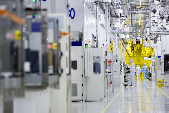
Since Samsung’s 5LPE uses more EUV layers than the company’s 7LPP process, expect it to be used on Samsung’s upcoming EUV fab in Hwaseong. The production line is set to cost 6 trillion Korean Won ($4.615 billion), it is expected to be completed in 2019, and start high volume manufacturing in 2020.
Related Reading:


13 Comments
View All Comments
PeachNCream - Tuesday, July 9, 2019 - link
Based on your response, it's clear that you're only interested in making ad-hominem attackes rather than focusing your citicisms on the points that Dragonstongue is making which is your own dumb fault since it's clear that you lack the ability to understand the content to begin with. It's people like you your grand conspiracy to commit large-scale censorship in order to violate peoples' right to type their thoughts into a box if they want just because you can't handle it.:D
Smell This - Tuesday, July 9, 2019 - link
"Samsung Foundry certified ... that these sets of tools meet Samsung Foundry’s requirements."
___________________________________
mmmm. Okay?
eastcoast_pete - Friday, July 12, 2019 - link
Foundries (like this one) don't design the chips, they "only" produce them. Whatever silicon is to be made by a foundry has to be first designed, usually by one of their many fabless clients, such as Apple, AMD, Huawei, IBM, Nvidia ...many more. (exception: Intel - both design and fabbing usually in-house, unless their fabs aren't up to it; Samsung's VLSI is kept separate from the foundry business to reduce foundry clients' fear of IP leakage). All these designs require tools (software), and any foundry worth it's salt will tell potential clients which software they validated for use with their manufacturing process. Samsung just did this for tools from Cadence and Synopsys for their newest process; if you design your chip with those (and know what you're doing), they guarantee they can fab them for you, provided you bring enough cash.