Samsung Unveils 6th Generation V-NAND Memory with Up to 136 Layers
by Anton Shilov on August 6, 2019 3:30 PM EST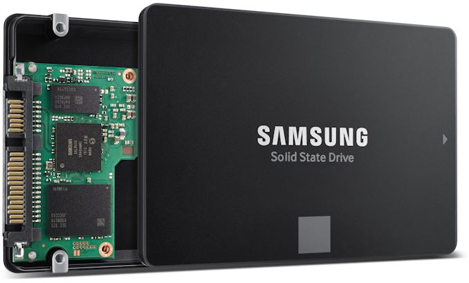
Samsung on Tuesday introduced its sixth-generation V-NAND memory, which in a bid to further improve capacity and density, features over 100 active layers. To make V-NAND with over 100 layers viable from performance point of view, the company had to use new circuit design technology. The new memory features 10% lower latencies and consumes 15% lower amount of power when compared to Samsung's previous-generation V-NAND.
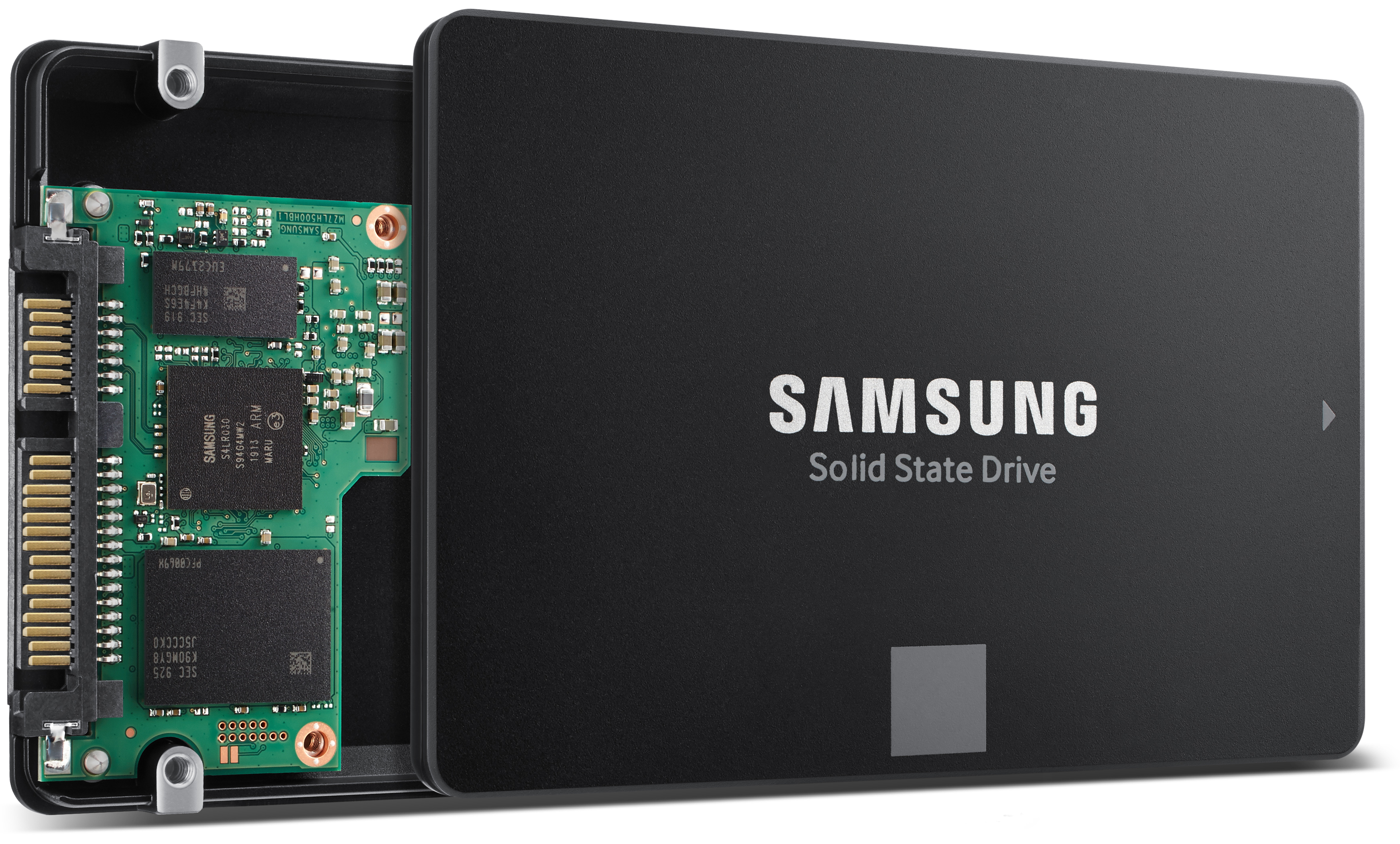
Samsung’s 6th Generation V-NAND features up to 136 layers as well as charge trap flash (CTF) cells. The new memory uses one stack and does not use technologies like string stacking to build over 100 layers. In order to ensure minimal errors and low latencies, Samsung had to use a new speed-optimized circuit design. The latter enables the new 3D TLC 256 Gb chips to offer below 450 microseconds (μs) latency for write operations and below 45 μs for read operations, which is 10% faster when compared to 5th Generation V-NAND, according to Samsung. Meanwhile, the latest V-NAND also features lower power consumption than its predecessors.
It is noteworthy that the new 256 Gb 136-layer V-NAND devices use 670 million holes, down from 930 million holes with the previous generation, which means that the new chips need fewer process steps and are easier to manufacture. What is important is that Samsung plans to use its 136-layer architecture with speed-optimized circuit design to build V-NAND devices with over 300 layers by mounting three of the current stacks on top of each other (thus tripling a chip’s capacity).
Initially, Samsung will offer 256 Gb 3D TLC 136-layer V-NAND devices that will first be used for Samsung’s 250 GB SSDs. Later this year Samsung intends to release 512 Gb 136-layer V-NAND devices that will be used for other drives as well as eUFS storage solutions.
Speaking of the 256 GB 6th Gen V-NAND SSD, it is important to point out that it uses Samsung’s new controller marked as the S4LR030/S94G4MW2.
Related Reading:
- Samsung Shares SSD Roadmap for QLC NAND And 96-layer 3D NAND
- Samsung's New 512 GB UFS 3.0 Chip for Galaxy Fold, Now in Mass Production
- Samsung Starts Production of 1 TB eUFS 2.1 Storage for Smartphones
- The Samsung 970 EVO Plus (250GB, 1TB) NVMe SSD Review: 96-Layer 3D NAND
Source: Samsung


41 Comments
View All Comments
Kjella - Tuesday, August 6, 2019 - link
Capacity is whatever they like, Samsung has a 30TB SSD in a 2.5" inch form factor. They scale almost linearly though, you can have 2x the capacity for 2x the price so there's really no advantage of buying in bulk, an 8TB SSD will be price of four 2TB SSDs.wanderer66 - Wednesday, August 7, 2019 - link
As long as the Cloud revolution continues, it will be a long time before prices take a dive. Demand has outstripped capacity for some time now, and will continue to keep prices relatively higher for some time to come.rpg1966 - Wednesday, August 7, 2019 - link
There's a massive advantage, i.e. how much capacity you can physically fit into your PC/NAS/pocket/etc.close - Wednesday, August 7, 2019 - link
The cost may increase quasi-linearly but the price usually doesn't. You pay a premium for the larger SSD simply because if you want to load up on storage you have to go for larger instead or more. Samsung (and not only) also knows.danielfranklin - Tuesday, August 6, 2019 - link
Thats where QLC will shine.Though personally i cant see why you wouldnt use a HDD for "archive" data, though that means different things to different people.
MrSpadge - Thursday, August 8, 2019 - link
Depends on your definition of semi-reasonable ;)brakdoo - Wednesday, August 7, 2019 - link
Anton, come on: these are 136 physical layers, NOT memory layers.You are forgetting about the dummy layers and the selectors. This would bring them much closer to the 128 mem layers everyone else is doing (and yes, those have those additional layers too, like every 3D NAND chip).
It could be even less than 128 like the chip they shown at ISSCC : https://thememoryguy.com/memory-sightings-at-isscc...
That's the reason Samsung is calling it 100+ layers or 1xx layers, not 136 layers: https://news.samsung.com/global/samsung-electronic...
Guspaz - Thursday, August 8, 2019 - link
Now if only Samsung didn't charge 2.5x as much as Intel for their same-size entry-level NVMe drives...MrSpadge - Thursday, August 8, 2019 - link
"It is noteworthy that the new 256 Gb 136-layer V-NAND devices use 670 million holes, down from 930 million holes with the previous generation, which means that the new chips need fewer process steps and are easier to manufacture."Anton, this number does not refer to the number of process steps, but rather to the number of holes etched into each 256 Gbit die, with each hole housing 100+ memory cells in the end. Cost decreases due to more dies per wafer, if higher processing cost don't outweight this (in which case they would not have started mass production).
uibo - Saturday, August 17, 2019 - link
"Initially, Samsung will offer 256 Gb 3D TLC 136-layer V-NAND devices that will first be used for Samsung’s 250 GB SSDs"Seriously? 250 GB 2.5'' SSD-s like the one on the picture? Haven't we moved past that capacity yet?