Kioxia: 3D Stacked Storage Class Memory, like 3D XPoint, Isn’t the Future
by Dr. Ian Cutress on December 30, 2019 2:00 PM EST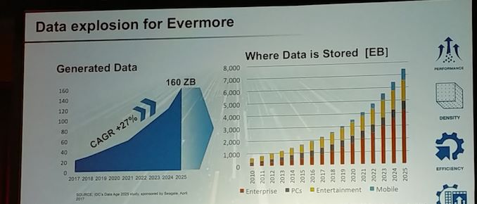
One of the key battlegrounds of the next decade is going to be storage: density, speed, and demand. Naturally all the major players in the space want to promote their own technologies of that of their competitors, and Kioxia (formerly Toshiba Memory) is no different. This year during their plenary talk at the International Electron Devices Meeting (IEDM) the company set forth its promotion of its BiCS flash product family, as well as its upcoming XL-Flash technology. What was interesting during this talk is a graph that seems to slam the long-term prospects of any of the upcoming Storage Class Memory (SCM) technologies like 3D XPoint from Intel and Micron.
Memory (DRAM) vs Storage (Flash) vs 'Storage-Class' Memory (SCM)
Memory at its basic level is having a property of a cell that can be calculated and converted into data. A simple DRAM cell contains electrons, and the presence / absence of electrons determine whether the value of that cell is a 1 or a 0. Flash storage memory has gone through several changes over the last couple of decades, with floating gate and charge trap technologies helping drive the manufacturing and scaling of storage. New types of memory are in various states of development/manufacture/shipping that rely on the resistance of the medium in the cell, or the spin of the medium in the cell, rather than the voltage.
Traditionally it is easy to think of each cell as a straight forward 0 or 1, on or off, with two distinct detection levels. However, depending on the type materials used, it can be possible to detect multiple levels within a single cell. The industry moved from 1-bit per cell (0 or 1) to 2-bits per cell (00, 01, 10, 11) to 3-bits per cell (000, 001, 010, etc) onwards, with the leading storage products now on four bits per cell and looking at even more than this. ‘DRAM’ time memory has always been a 1-bit per cell medium, however storage has been going through the motions of increasing the number of bits per cell. Moving to more bits per cell gets extra storage capacity, in effect, for ‘free’, however it requires the materials to have tighter tolerances and the detection circuitry to be more precise, and one way to do both of those is to increase the size of the cell, decreasing the density overall. The more bits per cell, the difficulty becomes in distinguishing between the property levels in 2 to the power of the number of bits. It’s an interesting conundrum.
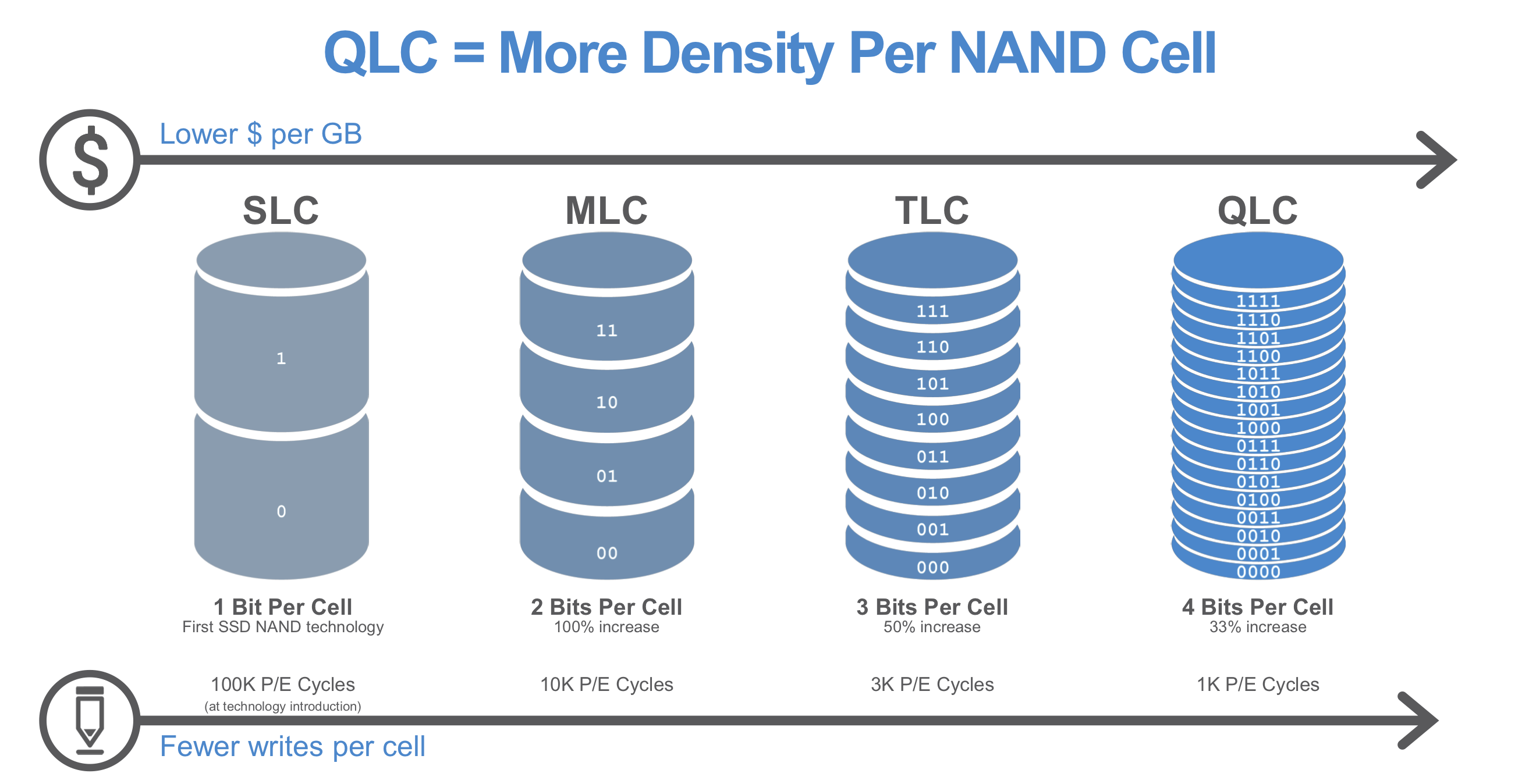
Kioxia’s current BiCS flash storage technology relies on stacking multiple layers of floating gate cells in a tower, and then repeating that design in the x-y directions to increase capacity. Kioxia currently ships a lot of 3-bit per cell and 4-bit per cell products, with the company looking at 5-bit per cell for special applications. The BiCs family of products has also been increasing the number of layers in its design, from 32 layer to 48 layer to 64 layer and now currently up to 96-layer, with 128+ layer in the future expected to arrive. Adding layers, by contrast to other methods, is fairly easy.
Kioxia is also building a new type of Flash called XL-Flash, which again adds another layer of parallelism to the concept of flash.

Storage Class Memory is slightly different to traditional flash memory. Memory works at a ‘bit’ level of access, while flash memory works at a ‘page’ and ‘block’ level. This means that while DRAM can access each bit and modify it, in flash it means that any write operation to the flash requires a whole page to be written at once. This means that every read-modify-write operation needs to read the full page, choose which bits are going to change, and re-write the page in full. This increases the wear on the drive (the number of read/write cycles), and there are many techniques in play in order to reduce the wear through wear levelling, spare storage area, and such. Memory by contrast needs to work at a bit level, and each bit needs to be selectable and adjustable – ‘storage class memory’ must therefore be able to act like memory at all times, and then be used for storage reasons when possible. The benefit of memory is meant to be its seemingly infinite (>10^18) cycle lifetime and low access latency, however it isn’t always that easy.
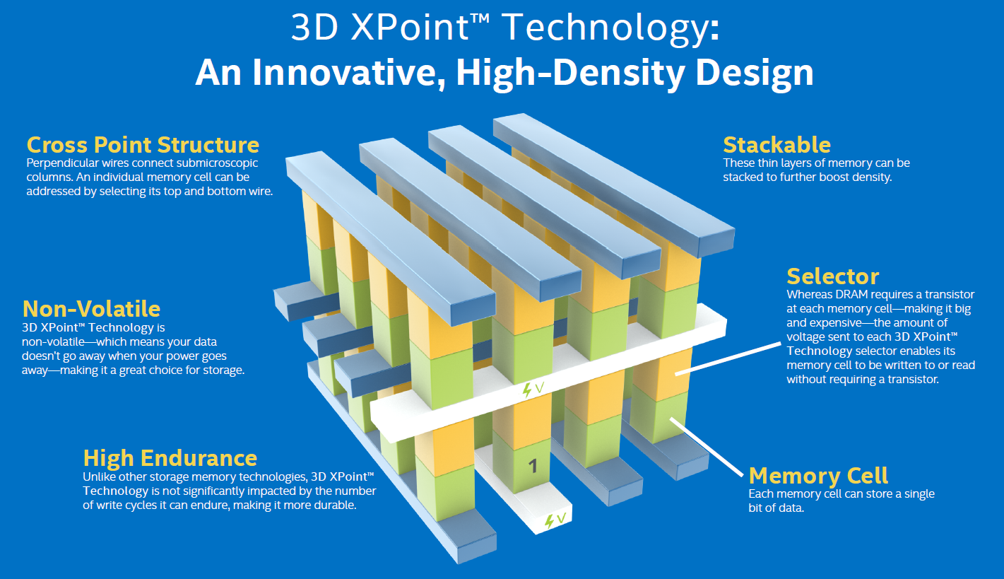
3D Stacked storage-class memory cells work a little different to flash. The easiest example here is 3D XPoint, which uses a phase change material to alter the resistance of a memory cell, and is accessed through an ovonic selector switch. The memory is built up through alternating the direction of word lines and bit lines to retain the bit-addressable nature of the SCM. In order to add more layers, the idea is that additional word and bit lines are added, along with the cells in-between.
Is 3D SCM the Future?
Why does Kioxia think that 3D Stacked SCM isn’t the future? I’ll go straight to the graph in question.

Here we have two lines showing relative cost per bit against the number of layers. Each line is normalized to a single layer of itself, not each other. The function that causes this graph is takes into account the number of layers (y-axis), the effective complexity of adding additional layers, the x-y area lost due to more complex control circuitry, and the yield lost by adding more layers. Putting numbers in spits out an effective cost-per-bit as the layers add up.
Now, 3D NAND is a proven technology. We have seen 90+ layers from multiple vendors in the market, and no-one is denying that adding layers is an effective way to go here, as the area loss is near to zero and the yield loss is similarly extremely low. This is because some of the etch-and-fill steps in the manufacturing process can cover many layers at once.
But for 3D Stacked SCM technologies, we still haven’t seen them expand beyond a single layer device in the market. Kioxia’s data shows that while its BiCS flash reduces down to an asymptotic value at cost per bit as we go past 10 layers, the company says that 3D Stacked SCM will at best only reduce to 60% of the cost per bit for a 4-5 layer device compared to a single layer – with the data rising from there. This is down to the increased cost per layer, the area loss required, and the yield decrease based on using complicated cell technologies that don’t have the benefit of decades of improvements. In order to build 3D Stacked memory, it's a painstaking process of layer upon layer, which leads to decreases in yield with each additional step.
For anyone interested, the equation for this graph is as follows:

Where n = the number of layers, Cf is the cost for the common layer, Cv is the cost per extra layer, A is the area penalty for adding a layer, and Y is the yield penalty for a single layer.
So it should be stated that at the plenary talk, we were not able to take photographs of the slides being presented. I made a quick note of the graph and the formula, and cycled back to Kioxia with suggested numbers for each of these variables to recreate these graphs. They replied saying I was very close with the following:
| Predicted Graph Values | ||||
| AnandTech | Cf Common Layer Cost |
Cv Extra Layer Cost |
A Area loss of Extra Layer |
Y Yield Loss of Extra Layer |
| NAND | 0.95 | 0.05 | ~0 | ~0 |
| 3D SCM | 0.70 | 0.30 | 0.02 | 0.06 |
When putting numbers in, it was clear that Cf + Cv had to equal 1, and as a result we basically end up looking at the ratio of the cost of adding a single layer to the design compared to the common layer of a design. The term involving area and yield affects the upswing of the curve, and the ratio of these ends up important for when the minimum value is as well as the rate at which the curve rises.
In the case of 3D SCM, the cost per bit at around 12 layers became the same as the cost per bit of a single layer, which is at the key of Kioxia’s commentary: if SCM was ever to hit the number of layers that NAND flash would, it would become prohibitively expensive (50x cost per bit of a single layer for a 64-layer SCM device).
Now of course, if we were to take the side of 3D Stacked SCM vendors, they will likely point out that just because of the price predictions today of >4 stacked layers seem cost-prohibitive, it doesn’t take into account what potential advancements will happen for the technology in the future. The ability to offer both high-density DRAM at order-of-magnitude performance levels or extremely low latency storage in a single product indicates its utility, rather than a lack of optimization for one or the other.
From what I’ve had the pleasure to work with, I can greatly see the benefit of SCM in the memory space – offering a super large pool of data to work from at a lower cost per GB than traditional DRAM, while also having a warranty that covers 100% access over the warranty period. As a storage medium, it offers an immediate fast access however the cost per GB is rather high. For storage at least, flash is going to be king of capacity for a long while yet.
Related Reading
- Toshiba Begins to Construct New BiCS 3D NAND Fab in Iwate Prefecture
- Kioxia Expands Automotive Grade eUFS Lineup: 512 GB for Extreme Conditions
- The Toshiba/Kioxia BG4 1TB SSD Review: A Look At Your Next Laptop's SSD
- Toshiba Memory To Rebrand As Kioxia
- Goke Unveils Toshiba XL-Flash-Based NVMe SSDs: Ultra-Low Latency
- Toshiba Launches XL-FLASH 3D SLC NAND
- Micron Finally Announces A 3D XPoint Product: Micron X100 NVMe SSD
- Intel Announces Optane Memory M15: 3D XPoint On M.2 PCIe 3.0 x4


23 Comments
View All Comments
Anymoore - Sunday, January 5, 2020 - link
proportional to the cell area, not pitch, but pitch^2WarthogARJ - Wednesday, July 22, 2020 - link
Very interesting.And do you have a reference for this?
As in it's a Kioxia researcher, but whom?
I imagine that by now there's something more he's done.
After all, Kioxia is still trying to sell things to other companies, so it needs to release some information.
WarthogARJ - Wednesday, July 22, 2020 - link
In addition, looking at the first graph, you can see where they want to focus on: Enterprise.In 2020, it's the largests secoctor, and they think it's going to almost triple in size 5 years.
Whereas, PC's was the smallest by far in 2020, and they think will grow faster, by maybe 4-5 times, but is still 2nd to last in size.
Entertaintainment and Mobile don't grow much.
So if you consider what Enterprise is replacing, HDD, it doesn't have to be anything very fancy in terms of speed relative to other SSD NAND, but better than the current HDD it's replacing.
So for either process, SCM or NAND flash, the main advantage of more layers wrt HDD, is COST, or I think more accurately, COST/"endurance units". And where it's different depending on the R/W ratio.
As far as that graph is concerned, I think it's misleading to use a single function for it as they've done. Or perhaps CLAIM to have done.
And especially to normalise everything, such that 1 layer of NAND cost = 1 layer of 3D SCM.
If you reconstruct the curves to be TOTAL cost as a function of layers, then it looks very different.
You get a very flat LINE for NAND, that shows a gradual rise in TOTAL cost as layers increase, but it's a VERY slow increase.
And you get a quite rapid increase in costs for layers, that tends to accelerate as you add layers.
And then, to adjust for the fact that SCM is currently more expensive than NAND, you need to add an offset, say make 1 layer of SCM = twice the cost of NAND.
So just add 1.0 to the SCM curve.
Then if you go back to the norrmalised bit cost by dividing by number layers, the two curves look VERY different.
The initial difference at one layer is indeed quite big, BUT, as you add layers, the 3D SCM cost per extra layer does NOT act the same, it CONTINUES to drop until 10 layers, and then does not rise very fast.
I cannot add a graph in Comments, but do it yourself and you shall see.
The point is that the Kioxia curves are misleading, because it depends very heavily on the cost per layer of each one. Assuming they are equal is NOT a "safe" assumption.
I doubt that they don't realise this, I think they are trying to push this point to sell the idea of using NAND flash for data centres for as long as they can. Its smoke and mirrors though.