AMD Ryzen Mobile 4000: Measuring Renoir’s Die Size
by Dr. Ian Cutress on January 14, 2020 9:00 AM EST- Posted in
- CPUs
- AMD
- Trade Shows
- Ryzen Mobile
- Renoir
- CES 2020
- Ryzen 4000
I’m pretty sure that the next time I go to a trade show where new silicon is being announced, the next tool I need in my backpack is a set of calipers in order to measure the die size. While die size doesn’t in of itself mean much as a number on its own, it is the end result of lots of hard work, focused co-design between silicon engineers and the semiconductor fabs, and ultimately there’s a fine balance between features, die size, performance, power, and at the end of the day, cost. With AMD showcasing the first x86-based 8-core CPU to move into the 15 W power envelope, finding out the die size is one of the elements of our investigation into how AMD has created its new Renoir / Ryzen Mobile 4000 product.
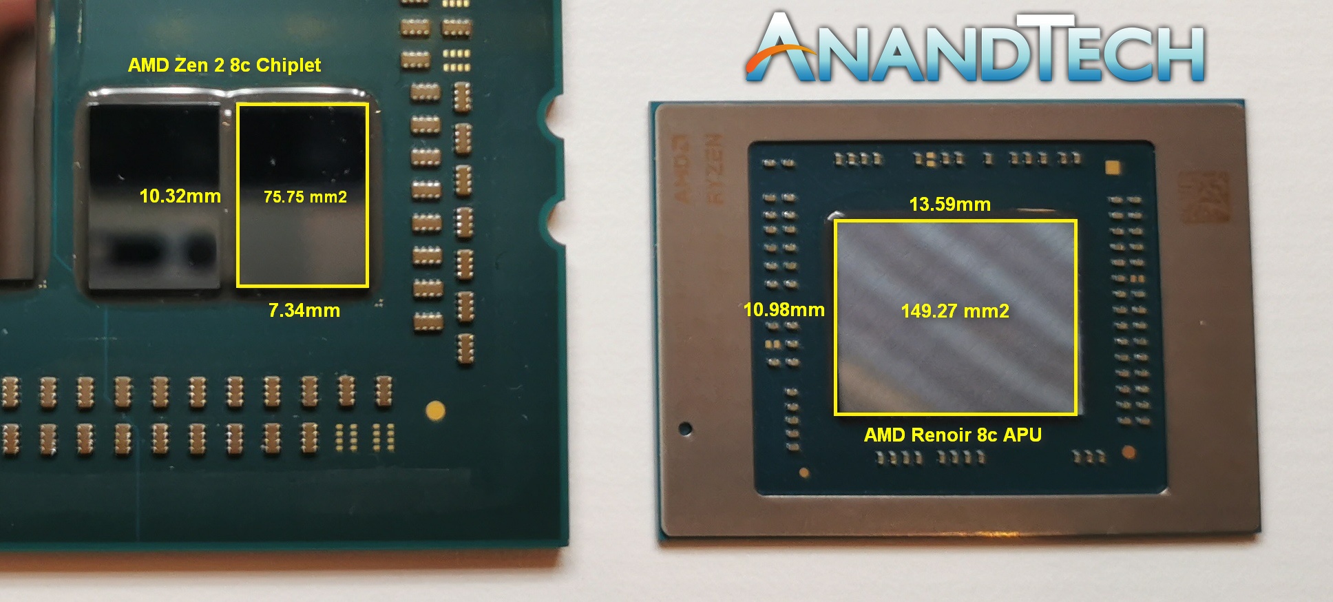
When I first saw the silicon, I wasn’t able to take pictures. Instead, I had to guess the size by manually placing it next to a 8-core Zen 2 chiplet from AMD’s monster 64-core Threadripper 3990X. We’ve known the die size for a while now, at 10.32 x 7.34 mm, or 75.75 mm2. My guess at the time that the new Renoir APU was almost exactly double the Zen 2 chiplet, and I mean it was scary how close to double the size it was. At the time of the announcement of Ryzen Mobile 4000, I had stated in our article that I estimated 150 mm2 for the die size. Turns out, I wasn’t too far wrong.
This image is not to scale.
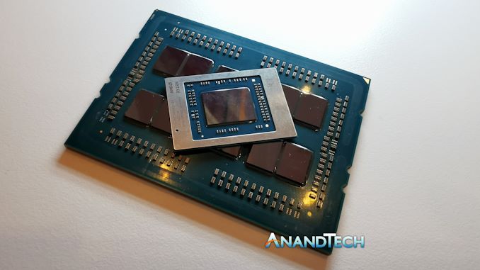
Later at CES, I went up to the AMD booth and this time they were more than happy for me to take photographs of the new silicon. The 3990X was also there, so I could place the two side by side and get a reasonable reference photograph on which to do calculations. This is the point of the event where I should have remembered to bring calipers! Taking photographs of chips is actually quite hard, making sure you get them lined up perfectly to get the same perspective, but also having enough light to get clear defined silicon edges.
In our picture, the Renoir chiplet you may notice is very slightly angled to the camera, which we’ve compensated for in our measurements.
With that in mind, here are our numbers.
The Zen 2 chiplet on the left, measures 10.32 mm by 7.34 mm, which is a ratio of 1.406 to 1.
In our image, the chiplet measured 265 pixels by 189 pixels, which is a ratio of 1.402 to 1.
In our image, the Renoir SoC measured 282 pixels by 350 pixels, which is a ratio of 0.806 to 1.
If we take the corresponding pixel dimensions, that gives us 10.98 mm by 13.59 mm, a ratio of 0.808 to 1.
This means that the die size of an eight-core Renoir APU with eight 2nd Gen Vega compute units, according to our calculations, 149.27 mm2.
| Die Sizes | ||||||
| AnandTech | x | y | Die Size | Process | Cores | EUs/ CUs |
| AMD Zen 2 Chiplet | 10.32 | 7.34 | 75.75 mm2 | TSMC N7 | 8 | - |
| Intel Ice Lake | 11.44 | 10.71 | 122.52 mm2 | Intel 10 | 4 | 64 |
| Intel Tiger Lake | 13.64 | 10.71 | 146.10 mm2 | Intel 10+ | 4 | 96 |
| AMD Picasso | 19.21 | 10.92 | 209.78 mm2 | GF 12 | 4 | 11 |
| AMD Renoir APU | 13.59 | 10.98 | 149.22 mm2 | TSMC N7 | 8 | 8 |
That’s pretty close to my 150 mm2 estimate, and I’ve also spoken to a few trusted individuals who have been tracking Zen 2 die structure sizes and graphics structure sizes, and they came out very similar, within 1mm2 or so.
At 149.27 mm2, assuming that AMD is achieving the same defect ratio on the silicon as reported by TSMC for the standard N7 process (0.09 defects per cm2), the process yield should be around 90%. Obviously that doesn’t take into account manufacturing for yield, or the distribution of the power/frequency of the chips within a wafer, but it’s still rather impressive.
Before AMD announced this new chip, there was a good deal of speculation as to how AMD would build it: either four cores with more graphics, or with eight cores and graphics only a little better. One factor of that was the die size: at 200 mm2, one would have expected AMD to definitely use eight cores. For sub 125 mm2, in order to maintain GPU performance, perhaps a quad-core design only have been suitable. However, AMD is claiming a great win here: eight Zen 2 cores, with frequencies at 1.8-4.3 GHz at 15 W, and despite fewer graphics compute units (down from 11 to 8), a higher per-compute unit performance claim of +56% means that performance is actually higher. All just shy of 150 mm2.
We are living in the future. I can’t wait for more.
It's worth noting that AMD's official number for the Zen 2 die size is 74 mm2. This is derived from the floorplan of the chip, which during manufacturing has additional space added to ensure clean die seperation between adjacent die prints. Ultimately what we get as the consumer is that seperation lane (known as a scribe lane) from one side of the die to the other, which is just slightly bigger than the floor plan that AMD supplies to the fabrication plant / TSMC. With calipers, what we get is that additional space, which is above AMD's quoted size.


103 Comments
View All Comments
Namisecond - Wednesday, January 22, 2020 - link
Do you have benchmarks showing 1050 levels of performance? Post a link so the rest of us can see then tooKorguz - Wednesday, January 22, 2020 - link
Namisecond, maroon1 wont post any links, cause there arent any, yet. this is their own personal opinion, with some personal bias thrown in, nothing more....Spunjji - Friday, January 24, 2020 - link
OP said "Would be nice to see..." - AKA "I'd like it if AMD did this...", not "AMD have done this".maroon1, on the other hand, made a performance claim that they can't back up. So maroon1 needs to justify that with evidence, whereas neither OP nor korguz have any such burden of proof.
Smell This - Friday, January 17, 2020 - link
Seems to me that there currently is a point of diminishing returns with the AMD APUs (sorry ... I'm going to keep calling it that, Dr Su !).Certainly on mobile, 8 CUs (512 shaders) seems to be the sweet spot. 10/11 CUs raises the performance bar, but not 1:1, and especially on the DT. Maybe DDR5 and Navi/RDNA-II can change the formula a bit, but a chiplet w/eDRAM (as a 4th level cache?) would be the logical long-term path ...
Namisecond - Wednesday, January 22, 2020 - link
You may be mistaking popularity by price for popularity by performance. I'd argue that 2200G/2400G sold well because they sold for a significantly lower price than their larger core count, GPU-less brethren. If the new desktop APUs sell at a similar price point, it should do well. Don't expect significantly better GPU performance from the 4000-series APUs over their older counterparts. Even 20% may be expecting too much.Gonemad - Thursday, January 16, 2020 - link
Huge chip areas at lower TDP = excellent cooling. Fantastic. Some bold manufacturers may even tinker with PASSIVE cooling?I mean, we are back on the 486 era, where chips only needed a heatsink. That's a full circle. I can see bold designs, with maybe just passive watercooling, or just a heatpipe plugging the thing into the aluminum case of the notebook, - turning it into a decent heatspreader - being feasible, without Apple levels of sacrifice to performance or durability.
Namisecond - Wednesday, January 22, 2020 - link
IIRC, 486 chips were right around 10W and I definitely recall my 486/33 system came with a fan for the heatsink. Even now, 10W TDP seems to be the tipping point where vendors consider active cooling for their products. My EDC laptop with a 6W TDP CPU makes do with a heat spreader plate, a big one. The 10W TDP desktop version of that same chip came with a fairly elaborate heatsink, sans fan. Anything 15W TDP and up will most likely come with active cooling or a very elaborate custom passive cooling setup.peevee - Monday, January 27, 2020 - link
They just need to start installing CPUs (and its LP memory, and M2 slots) into the screen half of the laptop, with ribbed aluminum as its cover. Much more cooling area where there is no keyboard, and even 2mm ribs with 2mm pitch increase the area by 3x again, easily.Namisecond - Wednesday, January 29, 2020 - link
Uh, no...unless you enjoy laptops that fall over backward when you open them up...jjjag - Wednesday, January 22, 2020 - link
The table is wrong. Ice Lake is 10+. The Canon Lake that was released in 2017 is the original 10nm. No idea if there is an official word, but wiki says Tiger Lake is 10++ and I think that is probably correct. I think it's also safe to assume that the slides you showed 2 years ago from Intel that had 10++ with a performance advantage over 10+ are now incorrect as Intel has probably changed direction in favor of manufacturability and lower power over raw performance