AMD Ryzen Mobile 4000: Measuring Renoir’s Die Size
by Dr. Ian Cutress on January 14, 2020 9:00 AM EST- Posted in
- CPUs
- AMD
- Trade Shows
- Ryzen Mobile
- Renoir
- CES 2020
- Ryzen 4000
I’m pretty sure that the next time I go to a trade show where new silicon is being announced, the next tool I need in my backpack is a set of calipers in order to measure the die size. While die size doesn’t in of itself mean much as a number on its own, it is the end result of lots of hard work, focused co-design between silicon engineers and the semiconductor fabs, and ultimately there’s a fine balance between features, die size, performance, power, and at the end of the day, cost. With AMD showcasing the first x86-based 8-core CPU to move into the 15 W power envelope, finding out the die size is one of the elements of our investigation into how AMD has created its new Renoir / Ryzen Mobile 4000 product.
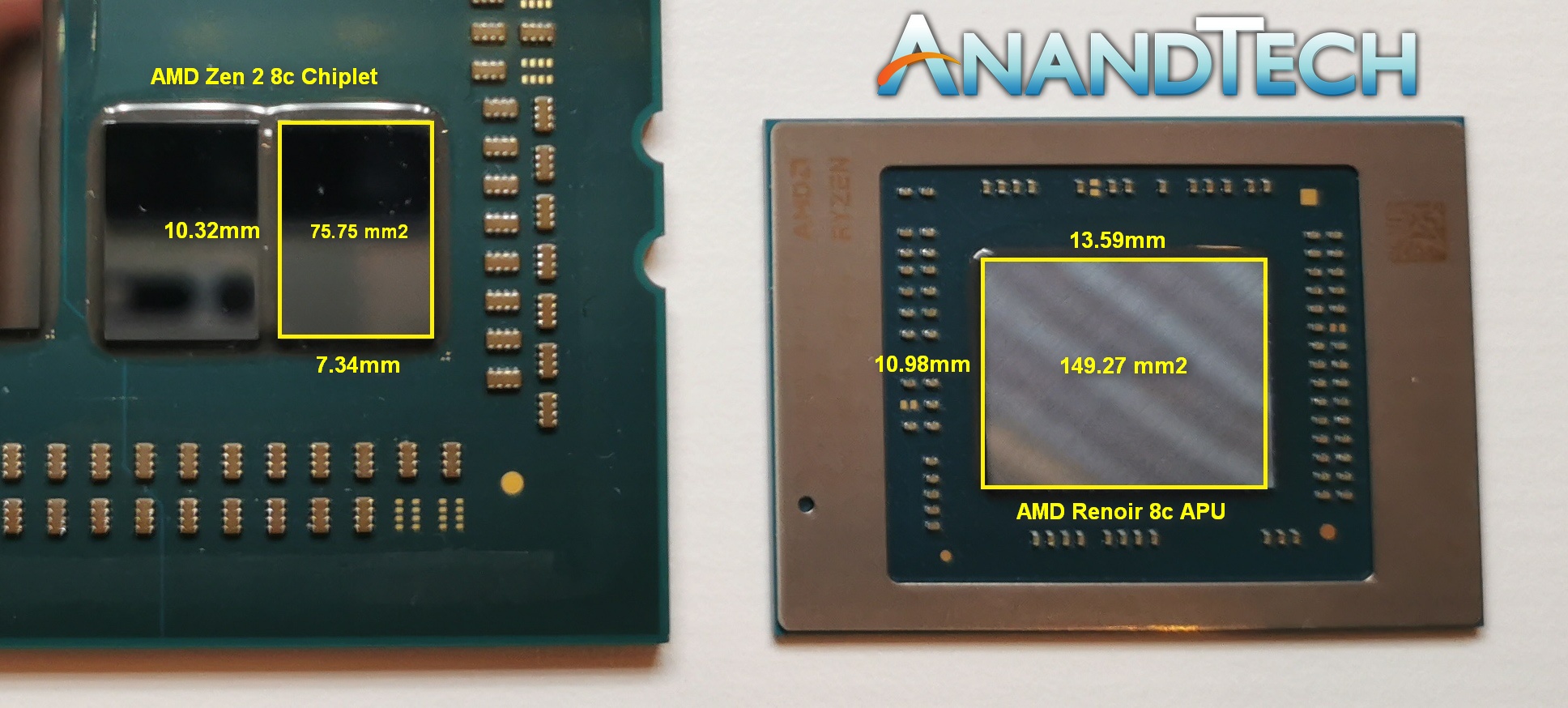
When I first saw the silicon, I wasn’t able to take pictures. Instead, I had to guess the size by manually placing it next to a 8-core Zen 2 chiplet from AMD’s monster 64-core Threadripper 3990X. We’ve known the die size for a while now, at 10.32 x 7.34 mm, or 75.75 mm2. My guess at the time that the new Renoir APU was almost exactly double the Zen 2 chiplet, and I mean it was scary how close to double the size it was. At the time of the announcement of Ryzen Mobile 4000, I had stated in our article that I estimated 150 mm2 for the die size. Turns out, I wasn’t too far wrong.
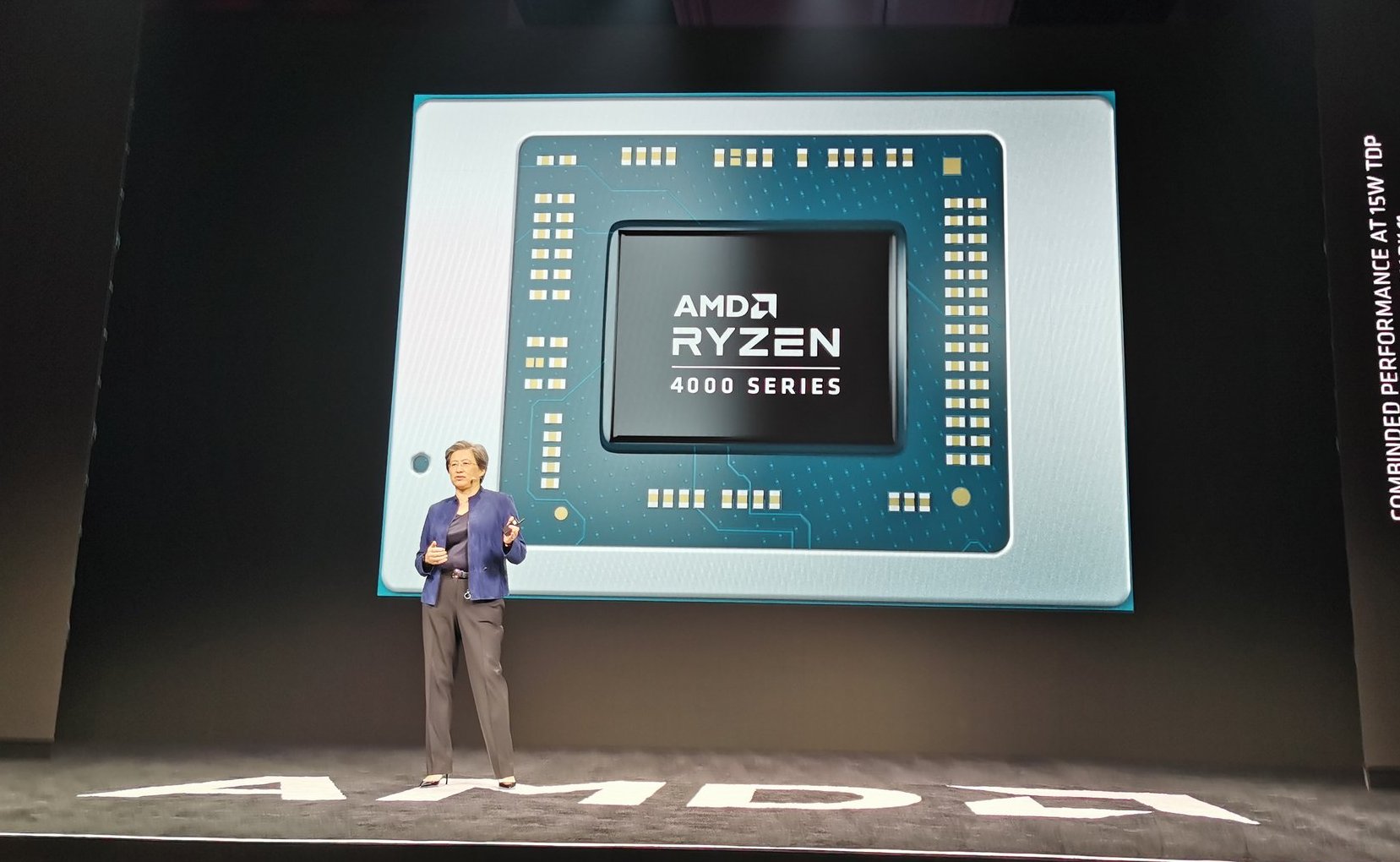
This image is not to scale.
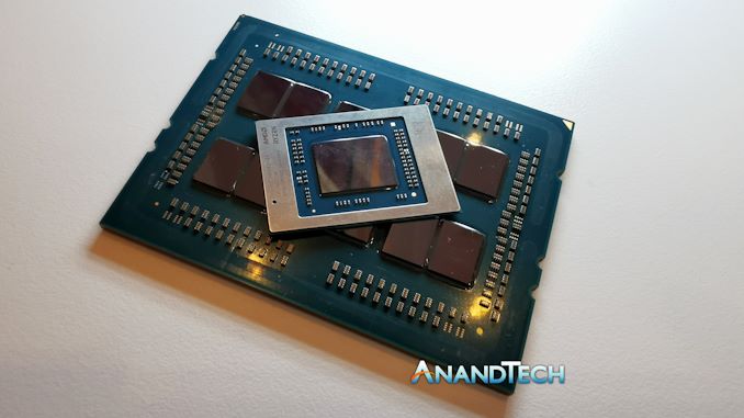
Later at CES, I went up to the AMD booth and this time they were more than happy for me to take photographs of the new silicon. The 3990X was also there, so I could place the two side by side and get a reasonable reference photograph on which to do calculations. This is the point of the event where I should have remembered to bring calipers! Taking photographs of chips is actually quite hard, making sure you get them lined up perfectly to get the same perspective, but also having enough light to get clear defined silicon edges.
In our picture, the Renoir chiplet you may notice is very slightly angled to the camera, which we’ve compensated for in our measurements.
With that in mind, here are our numbers.
The Zen 2 chiplet on the left, measures 10.32 mm by 7.34 mm, which is a ratio of 1.406 to 1.
In our image, the chiplet measured 265 pixels by 189 pixels, which is a ratio of 1.402 to 1.
In our image, the Renoir SoC measured 282 pixels by 350 pixels, which is a ratio of 0.806 to 1.
If we take the corresponding pixel dimensions, that gives us 10.98 mm by 13.59 mm, a ratio of 0.808 to 1.
This means that the die size of an eight-core Renoir APU with eight 2nd Gen Vega compute units, according to our calculations, 149.27 mm2.
| Die Sizes | ||||||
| AnandTech | x | y | Die Size | Process | Cores | EUs/ CUs |
| AMD Zen 2 Chiplet | 10.32 | 7.34 | 75.75 mm2 | TSMC N7 | 8 | - |
| Intel Ice Lake | 11.44 | 10.71 | 122.52 mm2 | Intel 10 | 4 | 64 |
| Intel Tiger Lake | 13.64 | 10.71 | 146.10 mm2 | Intel 10+ | 4 | 96 |
| AMD Picasso | 19.21 | 10.92 | 209.78 mm2 | GF 12 | 4 | 11 |
| AMD Renoir APU | 13.59 | 10.98 | 149.22 mm2 | TSMC N7 | 8 | 8 |
That’s pretty close to my 150 mm2 estimate, and I’ve also spoken to a few trusted individuals who have been tracking Zen 2 die structure sizes and graphics structure sizes, and they came out very similar, within 1mm2 or so.
At 149.27 mm2, assuming that AMD is achieving the same defect ratio on the silicon as reported by TSMC for the standard N7 process (0.09 defects per cm2), the process yield should be around 90%. Obviously that doesn’t take into account manufacturing for yield, or the distribution of the power/frequency of the chips within a wafer, but it’s still rather impressive.
Before AMD announced this new chip, there was a good deal of speculation as to how AMD would build it: either four cores with more graphics, or with eight cores and graphics only a little better. One factor of that was the die size: at 200 mm2, one would have expected AMD to definitely use eight cores. For sub 125 mm2, in order to maintain GPU performance, perhaps a quad-core design only have been suitable. However, AMD is claiming a great win here: eight Zen 2 cores, with frequencies at 1.8-4.3 GHz at 15 W, and despite fewer graphics compute units (down from 11 to 8), a higher per-compute unit performance claim of +56% means that performance is actually higher. All just shy of 150 mm2.
We are living in the future. I can’t wait for more.
It's worth noting that AMD's official number for the Zen 2 die size is 74 mm2. This is derived from the floorplan of the chip, which during manufacturing has additional space added to ensure clean die seperation between adjacent die prints. Ultimately what we get as the consumer is that seperation lane (known as a scribe lane) from one side of the die to the other, which is just slightly bigger than the floor plan that AMD supplies to the fabrication plant / TSMC. With calipers, what we get is that additional space, which is above AMD's quoted size.


103 Comments
View All Comments
outsideloop - Tuesday, January 14, 2020 - link
Ian, maybe you could comment on what Intel puts in the I/O chiplet of Ice Lake compared to what AMD has put in/left out of the Renoir chip?ksec - Tuesday, January 14, 2020 - link
>I had stated in our article that I estimated 150 mm2 for the die size. Turns out, I wasn’t too far wrong.Once you have eaten that many wafers, you can literally smell the die size XD
I was wrong in that AMD wanted to have GPGPU uArch in the iGPU, since Dr Su already stated there will RDNA in Ryzen Mobile in the future. But even with the current Ryzen Mobile, it doesn't look like Tiger Lake is attractive. It will be Quad CPU with AVX512, so it may be a better CPU but at half the Core, and Xe GPU I would bet it will be at best on par with AMD.
And then early next year you get AMD may be with Zen 2+ and RDNA2 ( Which is forms the basic of PS5 and Xbox X ) on TSMC N6.
But generally Speaking, despite everything that has happened over at Intel, and AMD being technically better in Desktop, Server and now Laptop, AMD is still not getting the market shares. I am disappointed in their sales, marketing, and forecasting department. Server is still a dismal 4%. Desktop CPU still under 20%. AMD needs to be a lot more aggressive especially in the Server Department which is where the big bucks are.
extide - Tuesday, January 14, 2020 - link
There is no Zen2+ (Why do people keep on about this..?)deksman2 - Tuesday, January 14, 2020 - link
Isn't AVX512 use relatively limited for consumers?Besides, AMD would easily retain the advantage with its increased core count and if software devs actually optimised their codes to take advantage of Zen uArch as it should.
That said, Zen2+ doesn't exist.
Zen 3 exists which will be a completely new architecture and produced on 7nm+ EUV node.
Also, Zen 3 should be released by the end of THIS year (2020) ... not early 2021.
2021 (most likely end of 2021) is slated for Zen 4 on 5nm (which seems to be on track because the yields have gone over 50% already).
sarafino - Tuesday, January 14, 2020 - link
Little use to most laptop consumers. Plus AVX512 is such a power hungry feature that it causes severe throttling to keep temperatures in control.IC asked Mark Papermaster if a Zen 2+ was planned in the future and Mark responded:
"MP: I have nothing to say on any refresh on current designs, but we always look at where it makes sense and where we’re able to take opportunities to provide a bump in performance, power, or die area."
So interpret that however you will. I don't see AMD squeezing in a Zen 2+ between Zen 2 and Zen 3, considering AMD has been pretty consistent with releases non their roadmap. Maybe Z2+ will live on in lower tier CPU's just as Z1/Z1+ has for the last year.
ash9 - Tuesday, January 14, 2020 - link
Very curious about the memory subsystem the Threadripper 3990X uses DMA to communicate to the GPU, and the 4000 chip look as if it does too, what's happening within the APU (oh it's not an APU anymore).Namisecond - Wednesday, January 22, 2020 - link
None of the Threadrippers have an on-die GPU, the 4000-series APU does. The more important question you should be asking is how does the 2000-series and 3000-series APUs communicate with their on-die GPUs?zamroni - Tuesday, January 14, 2020 - link
with 90% yield, most outcome will be the 16 thread 4800u. this is great news for laptop consumers.i just hope it has enough pci lanes to accommodate x4 thunderbolt port.
eva02langley - Tuesday, January 14, 2020 - link
Intel Ice Lake - 4 cores - 122.52 mm2AMD Renoir APU - 8 cores - 149.22 mm2
This should clear up the question about the density. Intel 10nm is clearly inferior to TSMC 7nm.
extide - Tuesday, January 14, 2020 - link
Well, 4 cores takes up about 25mm2 so 8c Ice Lake would be ~145mm2 they seem pretty on par actually -- depends on how much space the GPU takes on each but I wouldn't say it's clearly inferior.