Samsung Starts Production of 16 GB LPDDR5-5500 for Smartphones
by Anton Shilov on February 25, 2020 2:45 PM EST- Posted in
- Smartphones
- Memory
- Samsung
- Mobile
- LPDDR5
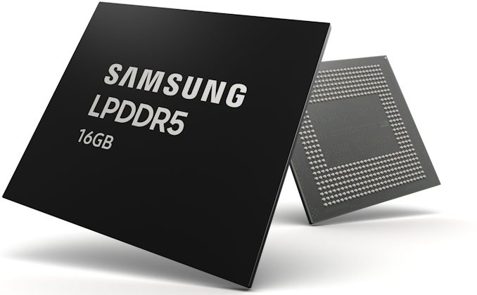
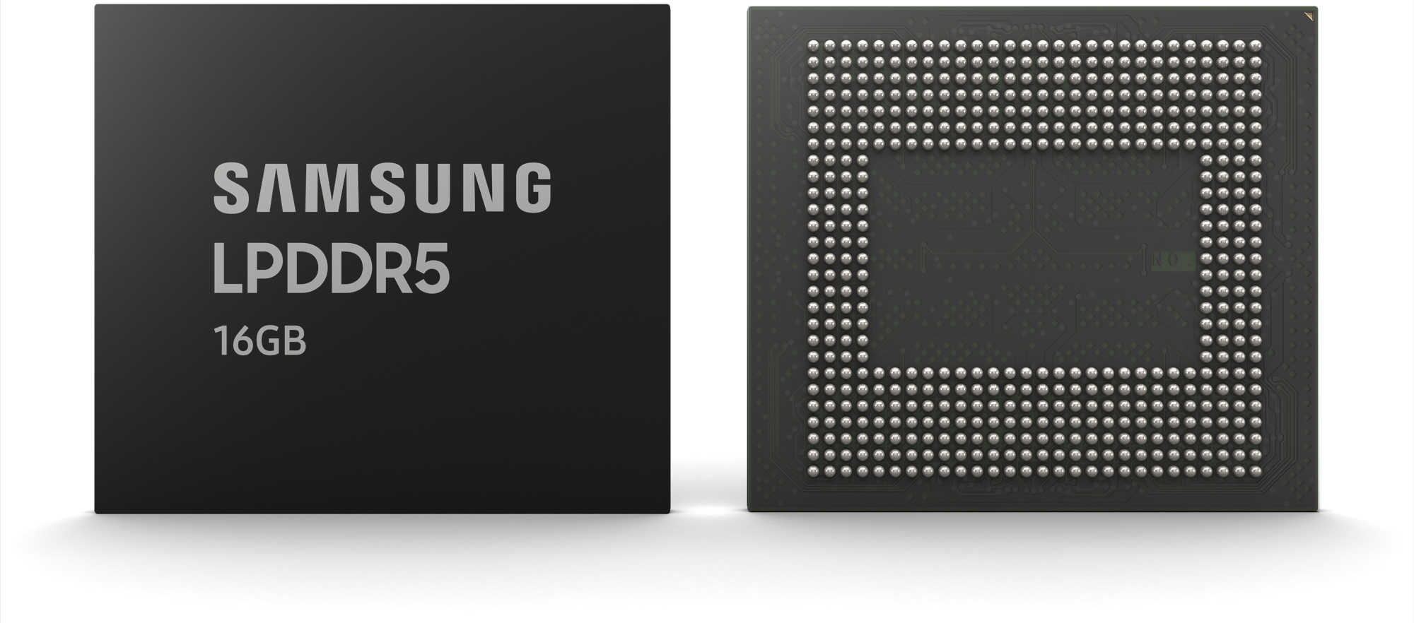
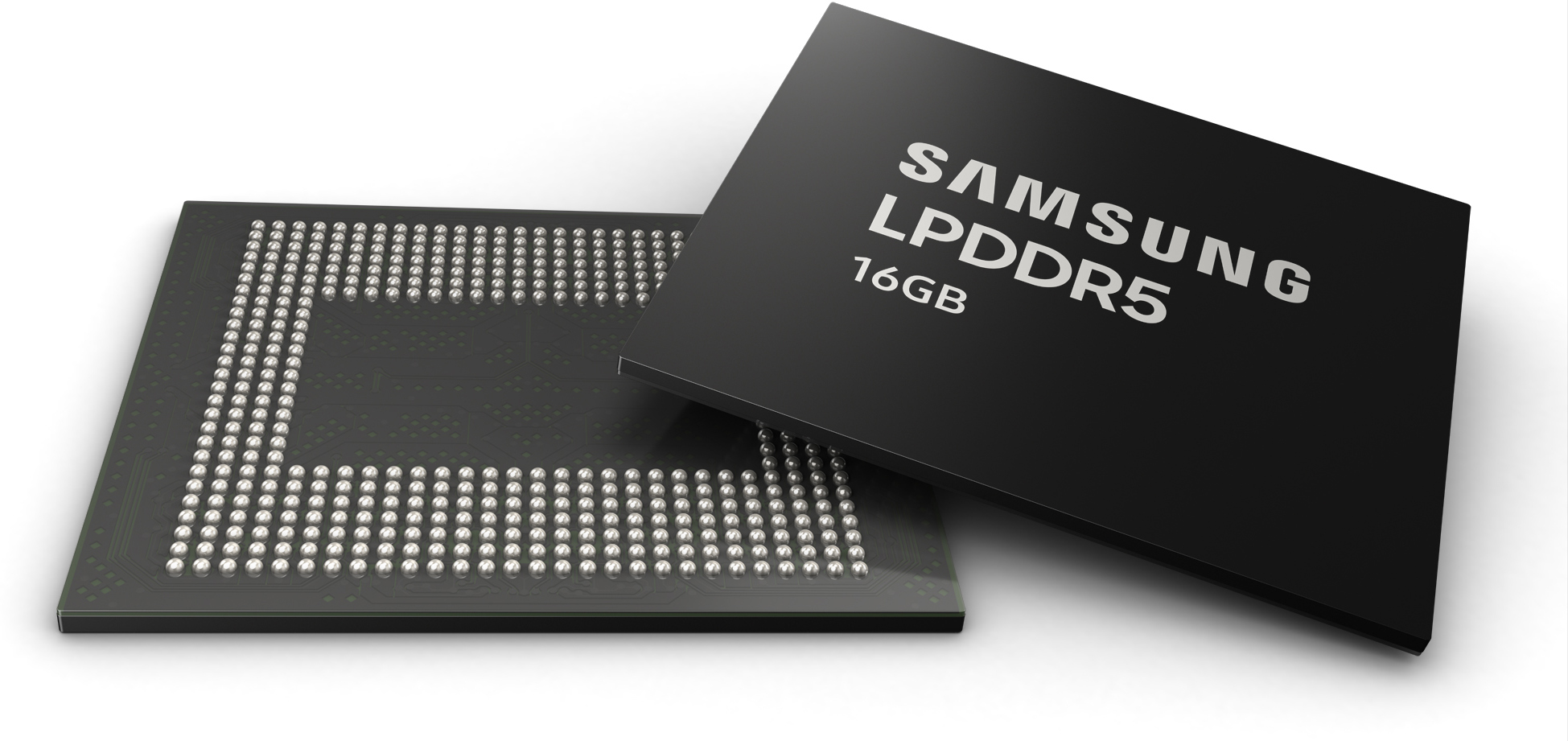
Samsung has begun mass production of the industry’s first 16 GB LPDDR5 memory for upcoming smartphones, such as the Galaxy S20 Ultra 5G handsets. The new DRAM devices not only offer higher capacity, but they are also 30% faster than previous-generation LPDDR4X-4266 used for previous-generation cellphones.
Samsung’s latest 16 GB LPDDR5 package consists of eight 12 Gb chips and four 8 Gb chips featuring a 5500 MT/s data transfer rate that can provide bandwidth of up to 44 GB/s. The very complex 12-device assembly is called a ‘mixed mode package’ because it contains DRAM devices that are accessed differently in different ranks. Samsung does not publish voltages of the new multi-chip 16 GB DRAM assembly, but only claims that it delivers more than 20% energy savings when compared to an 8 GB LPDDR4X package. Meanwhile, we do know that LPDDR5 memory chips feature a variable voltage that is up to 1.1 V.
The 12 Gb LPDDR5 devices are made using Samsung’s 2nd Generation 10 nm-class fabrication technology (also known as 1y nm), but the company does not disclose which manufacturing process is used to build 8 Gb LPDDR5 devices (though we are probably talking about 1y nm here as well).
Typically, DRAM makers make mass production announcements after they ship the first batch of products to a client. Considering that Samsung’s Galaxy S20 Ultra features 16 GB of LPDDR5 memory, it is more than reasonable to assume that it uses the company’s latest 16 GB LPDDR5-5500 DRAM package.
In the second half of this year Samsung plans to start production of 16 Gb LPDDR5 devices using its 3rd Generation 10 nm-class fabrication process (aka 1z). These chips will support speeds up to 6400 MT/s, but to take advantage of them Samsung will have to develop an SoC that supports such a high data transfer rate. Meanwhile, capacities of these upcoming LPDDR5 assembles remain to be seen.
Related Reading:
- Samsung Announces The Galaxy S20, S20+ and S20 Ultra: 120Hz, 5G, Huge Batteries, Crazy Cameras and $$$
- Micron Shipping LPDDR5 DRAM
- Samsung Starts Production of LPDDR5-5500 Devices: 12 GB of DRAM in a Smartphone
- Samsung Announces First LPDDR5 DRAM Chip, Targets 6.4Gbps Data Rates & 30% Reduced Power
- First with Snapdragon 865: ZTE Unveils Axon 10s Pro w/ 5G, 6.47-Inch AMOLED, 12 GB LPDDR5
Source: Samsung


33 Comments
View All Comments
danielfranklin - Tuesday, February 25, 2020 - link
And only half the battery life!azfacea - Tuesday, February 25, 2020 - link
I thought i already mentioned better power efficiency, but you dont seem to know whats going on here. signaling across the PCB is never more efficient than signaling that doesnt leave silicon. HBM is vastly more efficient than LPDDR5 in terms energy per bit. now if you are comparing 500GB/s to 50GB/s thats a different story. but you can always down clock HBM.I suspect the only reason we dont yet see HBM phones is cost and yield and lack of sufficient supply. not yet but should be soon.
brucethemoose - Tuesday, February 25, 2020 - link
Isn't HBM is an expensive, high power offering not built for mobile at all?Samsung developed more that one generation of "Wide I/O" which they more or less pitched as mobile HBM, but I'm not aware of any products that ever used it.
brucethemoose - Wednesday, February 26, 2020 - link
So looking into it more, Wide I/O was last talked about in 2016, and papers on similar standards have tapered off as well. IDK what happened, but I'd guess they hit some kind of roadblock.azfacea - Wednesday, February 26, 2020 - link
HBM is not high power its high bandwidth. if its more efficient with energy use per bit than its better than something thats less efficient. who are you to say "its not developed for mobile at all"now that doesnt mean you put 4 HBM stacks for 1TB/s bandwidth in a smart phone. it probably would have to have other changes as well, like slower refresh and others. the point i was making was that. i rather have 2.5D stacking in a phone than just increase capacity from 12GB to 16GB
thomasg - Wednesday, February 26, 2020 - link
You are mistaken.HBM uses 128-bit wide channels, while standard DDR uses 64-bit channels.
The whole point, and the main mechanism, behind LPDDR, as used in phones, is to use narrower channels, 16 or 32 bits wide, to save power.
The shorter signal lines HBM usually has going for it also do not apply - phones almost exclusively use package-on-package configurations for LPDDR, where lines are even shorter than in HBM setups.
Thus HBM is not more efficient per bit, it's about the same, or slightly worse. But HBM is _much_ worse when the high bandwidth is not required, as is the case most of the time for phones. That's where LPDDR has massive savings, and is - by far - the more efficient technology.
HBM in phones is absolutely pointless, when the huge bandwidth is not required (which it isn't).
azfacea - Friday, February 28, 2020 - link
yea you are probably right. i shouldnt have said HBM. I should have said, i prefer 3D stacking over more memory. It has to be a new technology to incorporate elements from HBM and LPDDR5danielfranklin - Tuesday, February 25, 2020 - link
Yeah im playing with you, semantics. Not saying samsung wont develop a "LP-HBM", but HBM2 isnt what you would want in your phone.Ultimatley all DRAM will likley end up over silicon at some point, for mobiles probably "via"d in through the top or bottom of the SOC.
Probably sooner than later too with the speed of mobile SOC dev.
azfacea - Wednesday, February 26, 2020 - link
yes definitely, sillicon stacking is coming to phones.deil - Wednesday, February 26, 2020 - link
yup. at least not ONLY HBM as phones are considered good with INSTANT responses not when they crunch 70 apps in background. And that is domain of DDR not HBM.