The Intel Comet Lake Core i9-10900K, i7-10700K, i5-10600K CPU Review: Skylake We Go Again
by Dr. Ian Cutress on May 20, 2020 9:00 AM EST- Posted in
- CPUs
- Intel
- Skylake
- 14nm
- Z490
- 10th Gen Core
- Comet Lake
Socket, Silicon, Security
Editor's note: this page is mostly a carbon copy of our deep-dive covering the Comet Lake 10th Gen announcement, with some minor tweaks as new information has been obtained.
The new CPUs have the LGA1200 socket, which means that current 300-series motherboards are not sufficient, and users will require new LGA1200 motherboards. This is despite the socket being the same size. Also as part of the launch, Intel provided us with a die shot:
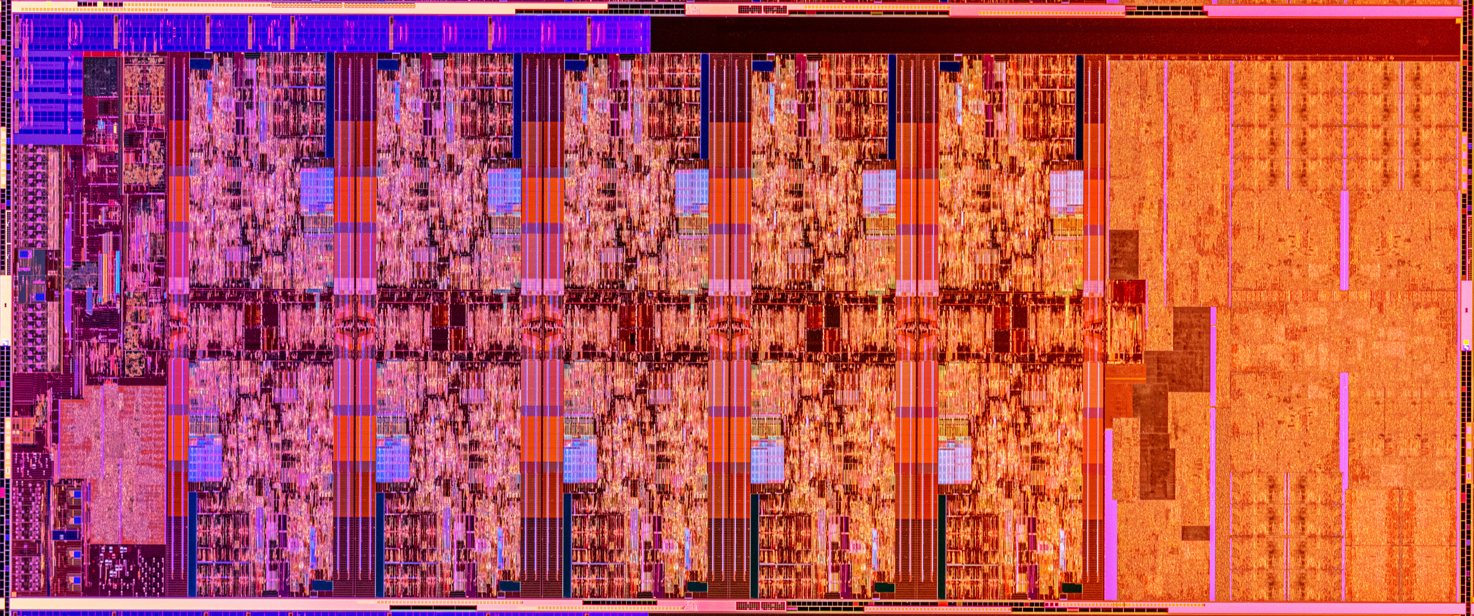
It looks very much like an elongated Comet Lake chip, which it is. Intel have added two cores and extended the communication ring between the cores. This should have a negligible effect on core-to-core latency which will likely not be noticed by end-users. The die size for this chip should be in the region of ~200 mm2, based on previous extensions of the standard quad core die:
CFL 4C die: 126.0 mm2
CFL 6C die: 149.6 mm2
CFL 8C die: 174.0 mm2
CML 10C die: ~198.4 mm2
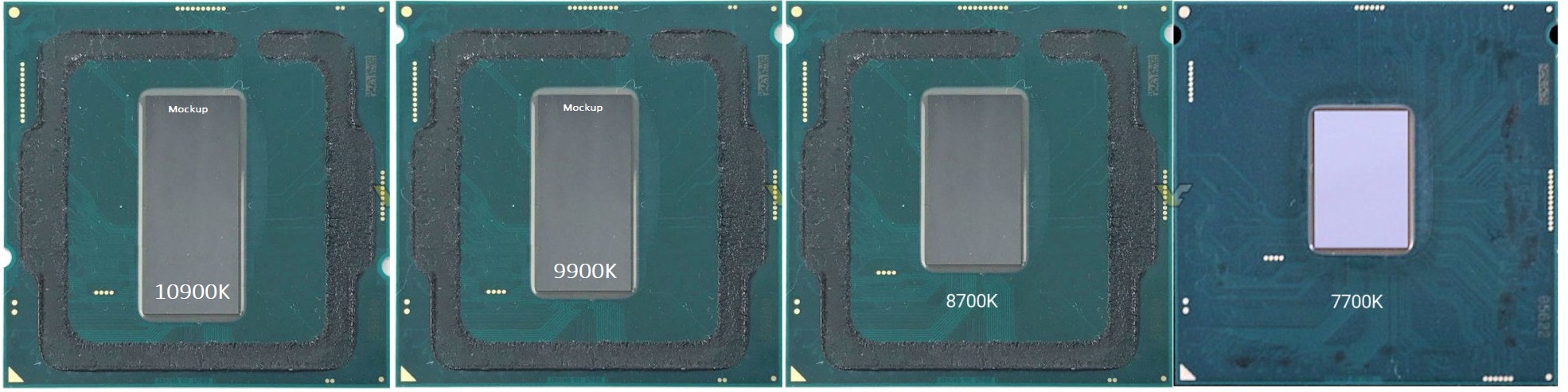
Original 7700K/8700K die shots from Videocardz
Overall, Intel is using the new 10C silicon for the ten core i9 parts, as well as for the eight core i7 parts where those get dies with two cores disabled. Meanwhile for the six core i5 parts, Intel is apparently using a mix of two dies. The company has a native 6C Comet Lake-S design, but they're also using harvested dies as well. At this point it appears that the K/KF parts – the i5-10600K and i5-10600KF – get the harvested 10C design, while all of the rest of the i5s and below get the native 6C design.
For security, Intel is applying the same modifications it had made to Coffee Lake, matching up with the Cascade Lake and Whiskey Lake designs.
| Spectre and Meltdown on Intel | ||||||
| AnandTech | Comet Lake |
Coffee Refresh |
Cascade Lake | Whiskey Lake |
||
| Spectre | Variant 1 | Bounds Check Bypass | OS/VMM | OS/VMM | OS/VMM | OS/VMM |
| Spectre | Variant 2 | Branch Target Injection | Firmware + OS | Firmware + OS | Hardware + OS | Firmware + OS |
| Meltdown | Variant 3 | Rogue Data Cache Load | Hardware | Hardware | Hardware | Hardware |
| Meltdown | Variant 3a | Rogue System Register Read | Microcode Update | Firmware | Firmware | Firmware |
| Variant 4 | Speculative Store Bypass | Hardware + OS | Firmware + OS | Firmware + OS | Firmware + OS | |
| Variant 5 | L1 Terminal Fault | Hardware | Hardware | Hardware | Hardware | |
Box Designs
Intel has again chanced the box designs for this generation. Previously the Core i9-9900K/KS came in a hexagonal presentation box – this time around we get a window into the processor.
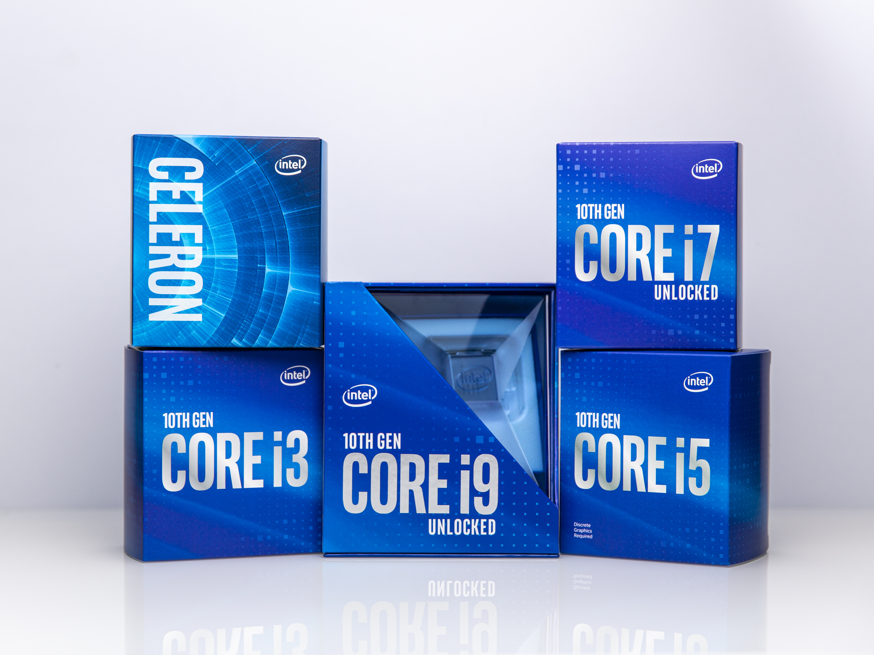
There will be minor variations for the unlocked versions, and the F processors will have ‘Discrete Graphics Required’ on the front of the box as well.
Die Thinning
One of the new features that Intel is promoting with the new Comet Lake processors is die thinning – taking layers off of the silicon and in response making the integrated heat spreader thicker in order to enable better thermal transfer between silicon and the cooling. Because modern processors are ‘flip-chips’, the bonding pads are made at the top of the processor during manufacturing, then the chip is flipped onto the substrate. This means that the smallest transistor features are nearest the cooling, however depending on the thickness of the wafer means that there is potential, with polishing to slowly remove silicon from this ‘rear-end’ of the chip.
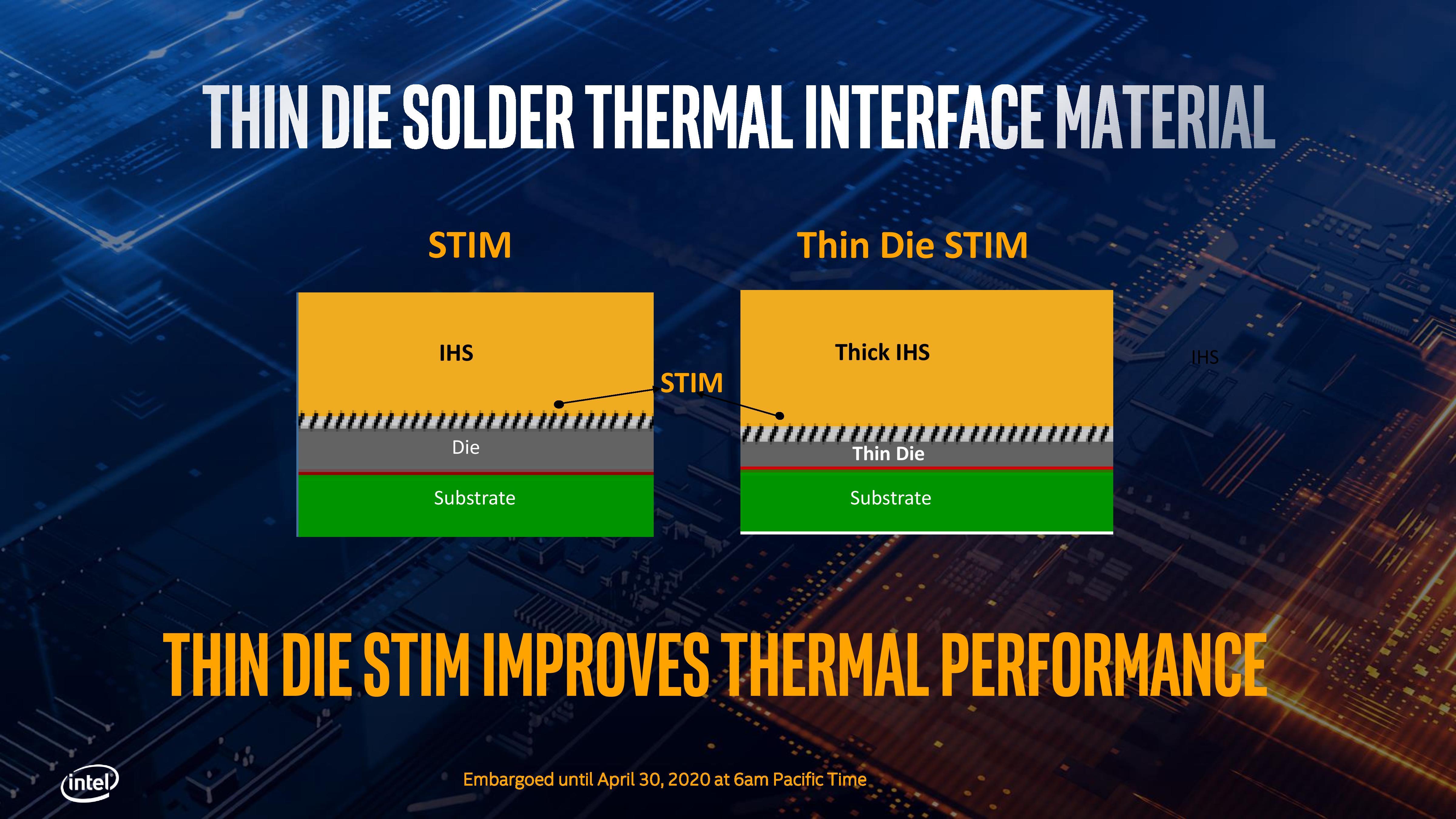
In this slide, Intel suggests that they apply die thinning to products using STIM, or a soldered thermal interface. During our briefing, Intel didn’t mention if all the new processors use STIM, or just the overclockable ones, and neither did Intel state if die thinning was used on non-STIM products. We did ask how much the die is thinned by, however the presenter misunderstood the question as one of volume (?). We’re waiting on a clearer answer.
Overclocking Tools and Overclocking Warranties
For this generation, Intel is set to offer several new overclocking features.
First up is allowing users to enable/disable hyperthreading on a per-core basis, rather than a whole processor binary selection. As a result, users with 10 cores could disable HT on half the cores, for whatever reason. This is an interesting exercise mostly aimed at extreme overclockers that might have single cores that perform better than others, and want to disable HT on that specific core.
That being said, an open question exists as to whether the operating system is set up to identify if individual cores have hyperthreads or not. Traditionally Windows can determine if a whole chip has HT or not, but we will be interested to see if it can determine which of my threads on a 10C/15T setup are hyperthreads or not.
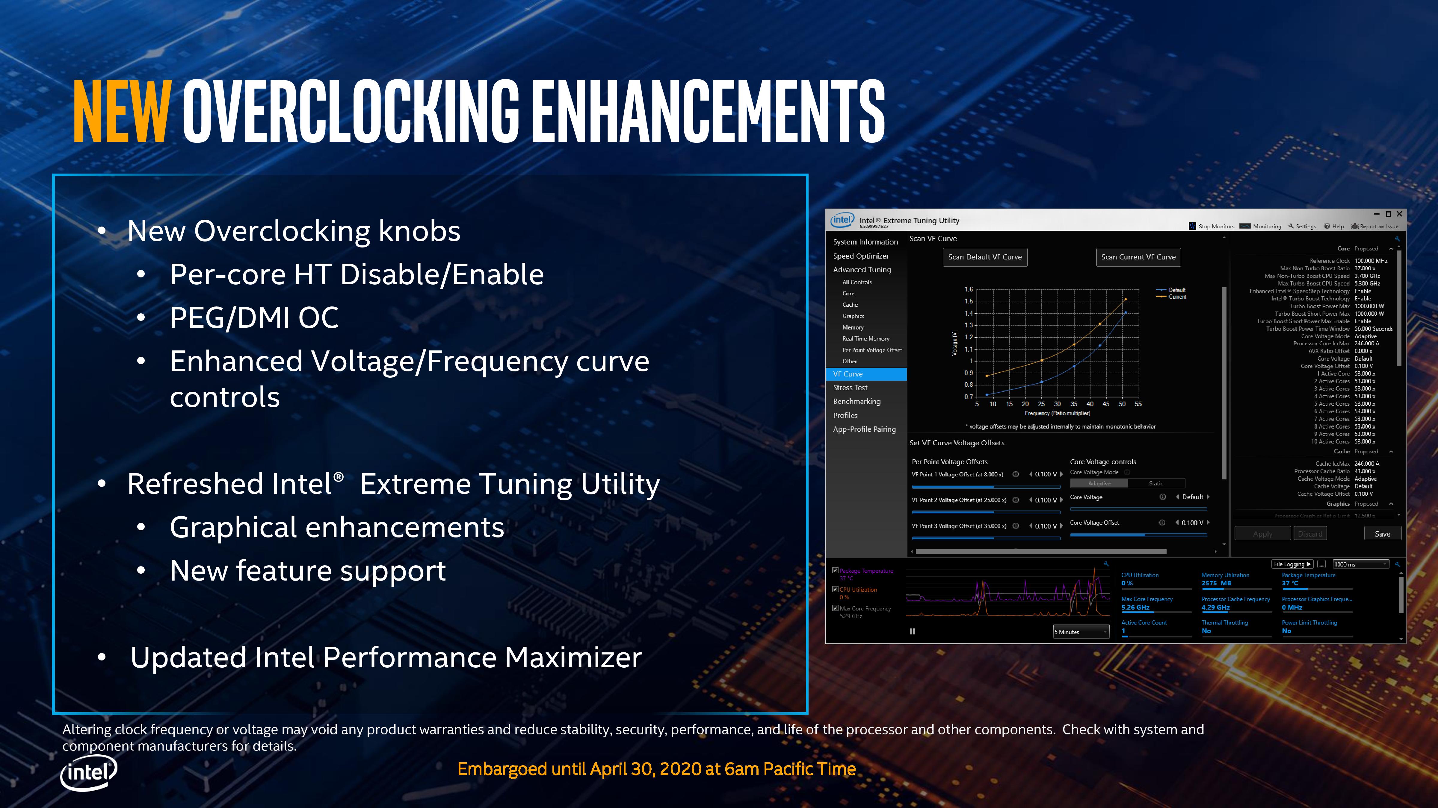
Also for overclocking, Intel has enabled in the specification new segmentation and timers to allow users to overclock both the PCIe bus between CPU and add-in cards as well as the DMI bus between the CPU and the chipset. This isn’t strictly speaking new – when processors were driven by FSB, this was a common element to that, plus the early Sandy Bridge/Ivy Bridge core designs allowed for a base frequency adjustment that also affected PCIe and DMI. This time around however, Intel has separated the PCIe and DMI base frequencies from everything else, allowing users to potentially get a few more MHz from their CPU-to-chipset or CPU-to-GPU link.
The final element is to do with voltage/frequency curves. Through Intel’s eXtreme Tuning Utility (XTU) and other third party software that uses the XTU SDK, users can adjust the voltage/frequency curve for their unlocked processor to better respond to requests for performance. For users wanting a lower idle power, then the voltage during idle can be dropped for different multiplier offsets. The same thing as the CPU ramps up to higher speeds.
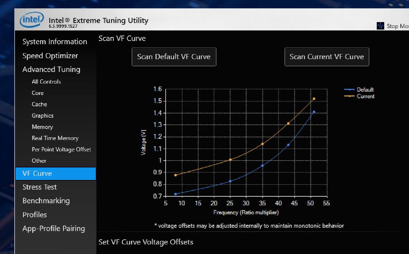
It will be interesting to see the different default VF curves that Intel is using, in case they are per-processor, per-batch, or just generic depending on the model number. Note that the users also have to be mindful of different levels of stability when the CPU goes between different frequency states, which makes it a lot more complicated than just a peak or all-core overclock.
On the subject of overclocking warranties, even though Intel promotes the use of overclocking, it isn’t covered by the standard warranty. (Note that motherboard manufacturers can ignore the turbo recommendations from Intel and the user is still technically covered by warranty, unless the motherboard does a technical overclock on frequency.) Users who want to overclock and obtain a warranty can go for Intel’s Processor Protection Plans, which will still be available.
Motherboards, Z490, and PCIe 4.0 ??
Due to the use of the new socket, Intel is also launching a range of new motherboard chipsets, including Z490, B460, and H470. We have a separate article specifically on those, and there are a small number of changes compared to the 300 series.

The two key features that Intel is promoting to users is support for Intel’s new 2.5 GbE controller, the I225-V, in order to drive 2.5 gigabit Ethernet adoption. It still requires the motherboard manufacturer to purchase the chip and put it on the board, and recent events might make that less likely – recent news has suggested that the first generation of the I225 silicon is not up to specification, and certain connections might not offer full speed. As a result Intel is introducing new B2 stepping silicon later this year, and we suspect all motherboard vendors to adopt this. The other new feature is MAC support for Wi-Fi 6, which can use Intel’s AX201 CNVi RF wireless controllers.

One big thing that users will want to know about is PCIe 4.0. Some of the motherboards being announced today state that they will support PCIe 4.0 with future generations of Intel products. At present Comet Lake is PCIe 3.0 only, however the motherboard vendors have essentially confirmed that Intel’s next generation desktop product, Rocket Lake, will have some form of PCIe 4.0 support.
Now it should be stated that for the motherboards that do support PCIe 4.0, they only support it on the PCIe slots and some (very few) on the first M.2 storage slot. This is because the motherboard vendors have had to add in PCIe 4.0 timers, drivers, and redrivers in order to enable future support. The extra cost of this hardware, along with the extra engineering/low loss PCB, means on average an extra $10 cost to the end-user for this feature that they cannot use yet. The motherboard vendors have told us that their designs conform to PCIe 4.0 specification, but until Intel starts distributing samples of Rocket Lake CPUs, they cannot validate it except to the strict specification. (This also means that Intel has not distributed early Rocket Lake silicon to the MB vendors yet.)
So purchasing a Z490 motherboard with PCIe 4.0 costs users more money, and they cannot use it at this time. It essentially means that the user is committing to upgrading to Rocket Lake in the future. Personally I would have preferred it if vendors made the current Z490 motherboards be the best Comet Lake variants they could be, and then with a future chipset (Z590?), make those the best Rocket Lake variants they could be. We will see how this plays out, given that some motherboard vendors are not being completely open with their PCIe 4.0 designs.


220 Comments
View All Comments
Ryan Smith - Tuesday, May 26, 2020 - link
To be sure, it's GTX 1080. IGP is the name of the setting.F123Nova - Saturday, May 23, 2020 - link
I am trying my best to be nice, but this article has the most dubious set of benchmarks I have seen, and the omission in the charts of Intel competition in certain charts where the competition is better makes me wonder why this article smells of a cash handout. Cant say for sure if this is another "Just buy it" piece, but it sure smells foul. I expected more from Anandtech...Ryan Smith - Tuesday, May 26, 2020 - link
Hi Nova,As has been the case for the past 23 years, we always strive to have accurate reporting, to the best of our abilities.
Given that we're in the process of rolling out some new benchmarks (such as the Crysis software render), we haven't yet had a chance to backfill in results for a number of processors. Unfortunately that's going to take some time. But in the meantime, was there any specific benchmark(s) you were concerned about? That might at least help us better prioritize what to backfill first.
And to be sure, there's no cash handout. That's not how we operate. (Selling out for anything less than an incredibly comfortable retirement isn't very helpful for our future employment prospects)
tvdang7 - Wednesday, May 27, 2020 - link
why couldnt AT use a 3800x instead of a 3700x.pcgpus - Friday, July 10, 2020 - link
Nice review. 10600K might be a new king in games (for fair price).If you want to compare this article with other services You have to go on this link:
https://warmbit.blogspot.com/2020/06/intel-core-10...
There are results from 9 services from 32 games!
After page load please pick up your language from google translate (right side of page).
pcgpus - Friday, July 10, 2020 - link
Nice review. 10900K is the new king in games!If you want to compare this article with other services You have to go on this link:
https://warmbit.blogspot.com/2020/06/intel-core-i9...
There are results from 9 services from 35 games!
After page load please pick up your language from google translate (right side of page).
Meteor2 - Wednesday, July 15, 2020 - link
A new microarchitecture doesn’t require a new process. When PAO immediately went south, I don’t understand why Intel didn’t just implement a new microarchitecture on 14 nm. Surely Ice Lake hasn’t taken four years to develop?Meteor2 - Wednesday, July 15, 2020 - link
*Sunny Cove. God Intel’s code-names are dumbmiss5tability - Saturday, August 8, 2020 - link
i just discovered this INTEL SCAM, now i dont freaking understand how those 10 gen cpu works i wanna buy i3 10300 and what im reading this is not 65W chip? what is real f@#%$@ power draw for those cpusdamian101 - Monday, August 10, 2020 - link
As far as I know Intel never used a single bidirectional ring bus on CPUs with more than 10 cores.On Intel Ivy Bridge CPUs with 12 and more (15) cores, Intel used three unidirectional ring buses. There were also no Sandy Bridge CPUs with more than 10 cores, and Intel used two bidirectional ring buses connected with buffered switches for their high core count Haswell CPUs.