Intel Launches Cooper Lake: 3rd Generation Xeon Scalable for 4P/8P Servers
by Dr. Ian Cutress on June 18, 2020 9:00 AM ESTSocket, Silicon, and SKUs
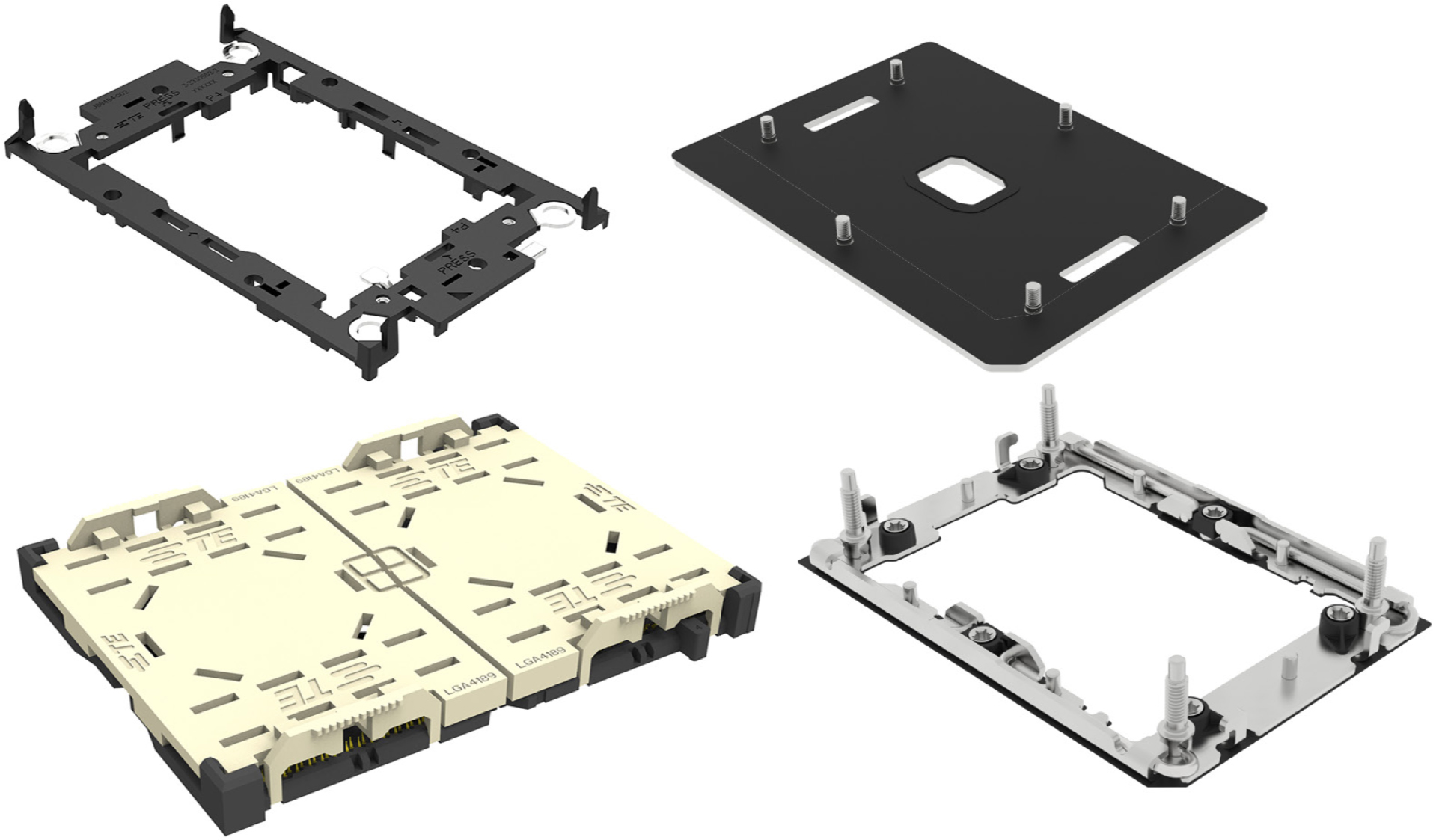
Cooper Lake Xeon Scalable ushers in a new socket, given that it is difficult to add in UPI links without adding additional pins. The new socket is known as LGA4189, for which there will be two variants: LGA4189-4 and LGA4189-5. When asked, Intel stated that Cooper Lake supports the LGA4189-5 socket, however when we asked an OEM about the difference between the sockets, we were told it comes down to the PCIe version.
LGA4189-5, for Cooper Lake, uses PCIe 3.0. LGA4189-4, which is for Ice Lake we were told, will be PCIe 4.0 Nonetheless, Intel obfuscates the difference by calling both of them ‘Socket P+’. It’s not clear if they will be interchangeable, given that technically PCIe 4.0 can work in PCIe 3.0 mode, and a PCIe 3.0 chip can work in a PCIe 4.0 board at PCIe 3.0 speeds, but it will come down to how the UPI links are distributed, and any other differences.
We've since been told that the design of the socket is meant to make sure that Ice Lake Xeon processors should not be placed in Cooper Lake systems, however Cooper Lake processors will be enabled in systems built for Ice Lake.
We’re unsure if that means that LGA4189 / Socket P+ will be a single generation socket or not. Sapphire Rapids, mean to be the next generation Xeon Scalable, is also set for 2nd gen Optane support, which could imply a DDR4 arrangement. If Sapphire Rapids supports CXL, then that’s a PCIe 5.0 technology. There’s going to be a flurry of change within Intel’s Xeon ecosystem it seems.
On the silicon side, Intel has decided to not disclose the die configurations for Cooper Lake. In previous generations of Xeon and Xeon Scalable, Intel would happily publish that it used three different die sizes at the silicon level to separate up the core count distribution. For Cooper Lake however, we were told that ‘we are not disclosing this information’.
I quipped that this is a new level of secrecy from Intel.
Given that Cooper Lake will be offered in variants from 16 to 28 cores, and is built on Intel’s 14nm class process (14+++?), we can at least conclude there is a ’28 core XCC’ variant. Usually on these things the L3 cache counts are a good indicator of something smaller is going to be part of the manufacturing regime, however each processor sticks to the 1.375 MB of L3 cache per core configuration.
This leads us onto the actual processors being launched. Intel is only launching Platinum 8300, Gold 6300, and Gold 5300 versions of Cooper Lake, given that its distribution is limited to four socket systems or greater, and to high scale OEMs only. TDPs start at 150-165 W for the 16-24 core parts, moving up to 205-250 W for the 18-28 core parts. The power increases come from a combination of slight frequency bumps, higher memory speed support, and double the UPI links.
| Intel 3rd Gen Xeon Scalable Cooper Lake 4P/8P |
||||||||||
| AnandTech | Cores | Base Freq |
1T Turbo |
DDR4 1DPC |
DDR4 2DPC |
DDR4 TiB |
TDP W |
4P 8P |
Intel SST |
Price |
| Xeon Platinum 8300 | ||||||||||
| 8380HL | 28C | 2900 | 4300 | 3200 | 2933 | 4.5 | 250 | 8P | No | $13012 |
| 8380H | 28C | 2900 | 4300 | 3200 | 2933 | 1.125 | 250 | 8P | No | $10009 |
| 8376HL | 28C | 2600 | 4300 | 3200 | 2933 | 4.5 | 205 | 8P | No | $11722 |
| 8376H | 28C | 2600 | 4300 | 3200 | 2933 | 1.12 | 205 | 8P | No | $8719 |
| 8354H | 18C | 3100 | 4300 | 3200 | 2933 | 1.12 | 205 | 8P | No | $3500 |
| 8353H | 18C | 2500 | 3800 | 3200 | 2933 | 1.12 | 150 | 8P | No | $3003 |
| Xeon Gold 6300 | ||||||||||
| 6348H | 24C | 2300 | 4200 | - | 2933 | 1.12 | 165 | 4P | No | $2700 |
| 6328HL | 16C | 2800 | 4300 | - | 2933 | 4.5 | 165 | 4P | Yes | $4779 |
| 6328H | 16C | 2800 | 4300 | - | 2933 | 1.12 | 165 | 4P | Yes | $1776 |
| Xeon Gold 5300 | ||||||||||
| 5320H | 20C | 2400 | 4200 | - | 2933 | 1.12 | 150 | 4P | Yes | $1555 |
| 5318H | 18C | 2500 | 3800 | - | 2933 | 1.12 | 150 | 4P | No | $1273 |
| All CPUs have Hyperthreading | ||||||||||
Quite honestly, Intel's naming scheme is getting more difficult to follow. Every generation of Xeon Scalable becomes a tangled mess of feature separation.
No prices are attached to any of the Cooper Lake processors from our briefings, but Intel did publish them in its price document. We can compare the top SKUs from the previous generations, as well as against AMD's best.
| Intel Xeon 8x80 Compare | ||||
| Xeon 8180M |
Xeon 8280L |
Xeon 8380HL |
AnandTech | EPYC 7H12 |
| Skylake | Cascade | Cooper | Platform | Rome |
| 14nm | 14+ nm | 14++ nm? | Node | 7nm + 14nm |
| $13011 | $13012 | $13012 | Price | ~$8500 |
| 28 C | 28 C | 28 C | Cores | 64 C |
| 2500 MHz | 2700 MHz | 2900 MHz | Base | 2600 MHz |
| 3800 MHz | 4000 MHz | 4300 MHz | 1T Turbo | 3300 MHz |
| 6 x 2666 | 6 x 2933 | 6 x 3200 | DDR4 | 8 x 3200 |
| 1.5 TiB DDR4 | 4.5 TiB Optane | 4.5 TiB Optane | Max Mem | 4 TiB DDR4 |
| 205 W | 205 W | 250 W | TDP | 280 W |
| 1P to 8P | 1P to 8P | 1P to 8P | Sockets | 1P, 2P |
| 3 x 10.4 GT/s | 3 x 10.4 GT/s | 6 x 10.4 GT/s | UPI/IF | 64 x PCIe 4.0 |
| 3.0 x48 | 3.0 x48 | 3.0 x48 | PCIe | 4.0 x128 |
| AVX-512 F/CD/BW/DQ |
AVX-512 F/CD/BW/DQ + VNNI |
AVX-512 F/CD/BW/DQ + VNNI +BF16 |
AVX | AVX2 |
The new processor improves on base frequency by +200 MHz and turbo frequency by +300 MHz, but it does have that extra 45 W TDP.
Compared to AMD’s Rome processors, the most obvious advantages to Intel are in frequency socket support, the range of vector extensions supported, and also memory capacity if we bundle in Optane. AMD’s wins are in has core counts, price, interconnect, PCIe count, and memory bandwidth. However, the design of Intel’s Cooper Lake with BF16 support is ultimately for customers who weren’t looking at AMD for those workloads.
We should also point out that these SKUs are the only ones Intel is making public. As explained in previous presentations, more than 50% of Intel's Xeon sales are actually custom versions of these, with different frequency / L3 cache / TDP variations that the big customers are prepared to pay for. In Intel's briefing, some of the performance numbers given by its customers are based on that silicon, e.g. 'Alibaba Customized SKU'. We never tend to hear about these, unfortunately.
Platform
As hinted above, Intel is still supporting PCIe 3.0 with Cooper Lake, with 48 lanes per CPU. The topology will also reuse Intel’s C620 series chipsets, providing 20 more lanes of PCIe 3.0 as well as USB 3.0 and SATA.
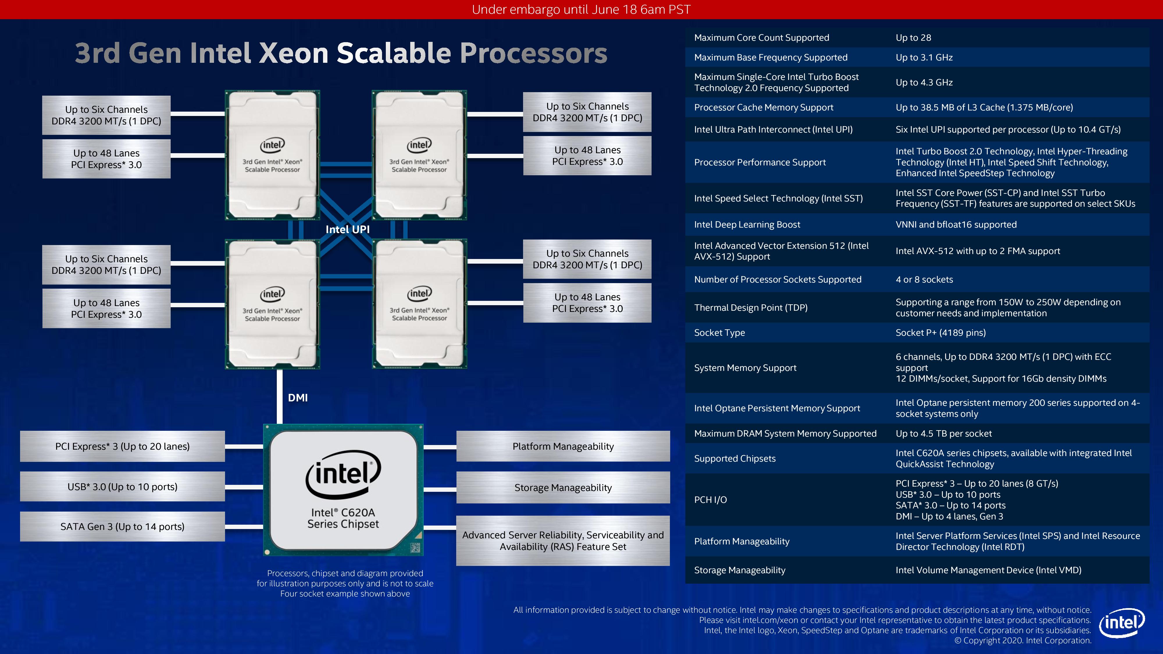
Intel did not go into items such as VROC support or improvements for this generation, so we expect support for those to be similar to Cascade Lake.


99 Comments
View All Comments
JayNor - Thursday, June 18, 2020 - link
Intel 4S and 8S also increase the memory bandwidth vs a 1S solution, since more memory channels per each socket, right?also ... Ice Lake Server will have Sunny Cove
from 12/12/2018 ARS Technica article:
"Both Intel and AMD have shared these limits since 2003. No longer: Sunny Cove extends virtual addresses to 57 meaningful bits (with the top 7 bits again either all zeroes or all ones, copying bit 56), with physical memory addresses of up to 52 bits. To handle this requires a fifth level in the page table. The new limits enable 128PB of virtual address space and 4PB of physical memory."
Deicidium369 - Friday, June 19, 2020 - link
Agreed - 2 dual socket is preferable to 1 quad socket.The comparison should be between the 2 socket Ice Lake SP and not the Cooper Lake 4 and 8 sockets. Ice Lake SP will be 38C per socket, 76 cores and 128 PCIe4 lanes in a dual socket system. Ice Lake's Sunny Cove brings a 20% increase in IPC - so that 76C performs more like a 90 or 91 core Cooper Lake. So 128 AMD cores vs 90 Intel cores - and the same 128 PCIe4 lanes and the same 8 channel memory - and the ability to use Optane DIMMs
Not much of an advantage anymore.
schujj07 - Friday, June 19, 2020 - link
Due to VMware's change in licensing, no one is going to buy a 38c Ice Lake same as no one will buy a 48c Epyc. The only people who might are cloud providers running open source hypervisors. IDK if you know how the licensing changed, but VMware has changed their license to 32c/socket/license. If you are running a 38c Ice Lake you will need 2 licenses for it, same as the 48 or 64c Epyc. The difference is the 64c Epyc at least maximizes the cores/socket requirement.When Ice Lake is released, it won't be competing against Zen2 Epyc, it will be competing against Zen3 Epyc.On the PCIe lane Ice Lake is still at a disadvantage in a dual socket setup. Depending on configuration, Epyc can have 160 PCIe 4.0 lanes for IO and still have 96 lanes for CPU-CPU communication. Even with 96 CPU communication lanes EPYC still provides ~50% more CPU-CPU bandwidth than an Ice Lake with 6 UPI links. In all honesty Ice Lake only has caught up with 1st Gen Epyc on IO but 2nd Gen on IPC.
Deicidium369 - Saturday, June 20, 2020 - link
Intel will sell as many ICL 38 cores as it can produce - I agree that most will be 32C IF they are destined for a VMware farm..Epyc has 128 PCIe4 Lanes PERIOD. in a dual socket Epyc - 64 lanes on EACH CPU is used to communicate with the other CPU. Leaving 128 PCIe4 lanes for IO. and 64 PCIe4 lanes for CPU to CPU communications..
Cool story
schujj07 - Saturday, June 20, 2020 - link
Wrong. There are 2 different dual socket setups possible. The 128 lane IO lane setup and the 160 lane IO setup. https://www.servethehome.com/amd-epyc-7002-series-... In the 128 IO setup there are also 128 lanes for Cpu-CPUDeicidium369 - Saturday, June 20, 2020 - link
There are no 4 socket Epycs.each CPU has 128 PCIe4 lanes - in a 2 socket system, 64 of them are used as CPU to CPU communications - please explain how you can add additional processors and still have PCIe lanes for, you know, IO.
AnGe85 - Thursday, June 18, 2020 - link
As you can already estimate/derive from the provided graph, Epyc does not compete with Xeon's in DL/ML-Tasks, simply because of missing features.A 4S system based on low priced Xeon's should already be enough to outperform a high-end Epyc system with two 7742. AVX-512, VNNI and DLBoost provide a much higher relative performance due to specialization for these types of workloads.
AMD will provide semi custom Zen3-Epyc's for the Frontier with good cause. ;-)
mode_13h - Thursday, June 18, 2020 - link
But, if you really care about deep learning performance, then you wouldn't use a CPU for it. That's why Intel just spent $2B to acquire Habana Labs.Deicidium369 - Thursday, June 18, 2020 - link
Or FPGAs configured as Tensor cores or tensor coresmode_13h - Thursday, June 18, 2020 - link
Also, AVX-512 has significant performance pitfalls. It's close to being an anti-feature.