Intel Roadmap Update: Alder Lake In H2’21, Ice Lake-SP Late This Year
by Ryan Smith on July 23, 2020 11:15 PM EST- Posted in
- CPUs
- Intel
- Ice Lake
- Sapphire Rapids
- Alder Lake

Among several different updates tucked into Intel’s Q2’2020 earnings report, the company included a brief update on some of their future products. While the bulk of the company’s focus is currently on their next-generation Tiger Lake CPUs, which are launching this quarter, the company is also looking at what comes after Tiger Lake, as well as the future of their highly profitable server business.
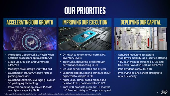
First off, Alder Lake has finally been formally outed. The successor to Tiger Lake now has an official launch window of the second-half of 2021. The 10nm chip will be for both mobile and desktops, making it the first 10nm chip that Intel has confirmed will come to desktops. Very little is otherwise officially known about the chip, but Intel’s ISA documents have previously revealed that there will be some new instructions found in that chip.
Otherwise the six-month window for kicking off production shipments is a fairly wide one for a chip that doesn’t rely on a new process node. Intel product cycles are rarely under a year long, so at first blush we’d be surprised if this was anything earlier than a late 2021 product. But with Intel’s recent 7nm delay and planned ramp-up of their 10nm process, it may be that Intel will be trying to pull it in and launch it in Q3, similar to this year’s Tiger Lake launch.
Meanwhile on the server side of matters, Intel is preparing for both Ice Lake-SP as well as its successor, Sapphire Rapids. One of the many victims of Intel’s 10nm woes, Ice Lake-SP is Intel’s first 10nm server chip. As of late the company has been riding a wave of profitability based on its server parts, so a newer part that improves on core counts and energy efficiency will be a welcomed addition to Intel’s product lineup, not to mention better able to fend off AMD’s powerful EPYC “Rome” processors.
Initial production shipments for Ice Lake-SP are set to start by the end of this year. Though Intel’s language is loose enough that this may mean that larger volumes of the chip may not ship until 2021.
Following Ice Lake-SP will be Sapphire Rapids, Intel’s second-generation 10nm server part. Along with getting Intel’s product release cadence closer to being back on track, Sapphire Rapids will play an important role in unifying Intel’s split Xeon families. Intel’s oddball 14nm Cooper Lake Xeons, which are currently shipping, support bfloat16, but Ice Lake-SP will not. For 10nm chips that support is finally being rolled into Sapphire Rapids, making the new chip the successor to both Cooper Lake and Ice Lake-SP in every way.
Sapphire Rapids will follow Ice Lake-SP by roughly a year. According to Intel’s presentation deck, chips will begin sampling in H2’2020, while CEO Bob Swan’s prepared remarks state that initial production shipments will begin at that time.
What follows these chips, in turn, will be the big question that Intel is currently wangling with in light of their 7nm delay. The company has made it clear that they intend to maintain an annual release cadence, divorced from their process roadmap if necessary. Depending on the state of their 7nm process, that may mean 7nm chips, 10nm chips, chips using dies from both processes, or even using dies from third-party fabs. Intel has opened the door to all possibilities, and their 2022 chips will likely be their first chance to embrace their new pragmatic approach.
Source: Intel


64 Comments
View All Comments
0ldman79 - Sunday, July 26, 2020 - link
They can put memory on package but that will impact thermals.They can't put memory slots on the package without making the package a board. By the time they make it a board it's literally the exact same thing it is today on the motherboard, literally the first hop out of the CPU socket. Memory latencies have nothing to do with the current layout. The only way to improve that would be to go do a different type of memory, HBM on package as an L4, something like that. DDR5 does show promise, splitting the channels won't directly help the latency but giving 4 channels will give twice the chance of not having to wait on the memory that's in the middle of another process.
dotjaz - Monday, July 27, 2020 - link
You forgot EM wave travels at limited speed, a typical wiring would add 2-3nspeevee - Monday, July 27, 2020 - link
Today the package is already a board. The chip itself takes a tiny part of the space since after 8080 or so.Santoval - Sunday, July 26, 2020 - link
"capped at 5GHz (either overclocked, or now mainstream parts)".There used to be a clear distinction, but after Zen was released Intel could no longer compete in IPC so they started overclocking their mainstream parts, which they still do. This is why their TDP values have gone through the roof.
jospoortvliet - Monday, July 27, 2020 - link
sure, they compete by clocking higher at higher top, but it gives them the crown (well in some situations) and i guess that is what matters. Amd couldn't clock their cpus higher even when allowing tdp to blow so intel has at least some advantage there. If they had brought a newer arch to 14nm 3 years ago and another last year the world would have looked different: amd would be well behind. Certainly bad management at Intel to take the risk assuming your process never delays (...), but given the delays the gap is surprisingly small....Spunjji - Friday, July 24, 2020 - link
1) Intel 14nm is really not directly comparable to GloFo 14nm (Intel's process is markedly superior).2) Zen's clock speed deficits are partially a result of the design of the architecture, which is why Zen+ only provided incremental improvements on that front even though it was much more heavily tailored to 14nm.
You're certainly right that it's not just the manufacturing process that makes a good CPU, though.
Santoval - Sunday, July 26, 2020 - link
"Zen's clock speed deficits are partially a result of the design of the architecture"Only partially, but we don't know how partially. Still, everything else being equal smaller nodes beyond a certain point result in lower clocks. If Zen 2 had been fabbed with TSMC's highest transistor density at 7nm (~97 MTr/㎟) its clocks would have been even lower (while its energy efficiency would be even higher).
0ldman79 - Sunday, July 26, 2020 - link
I think it's fair to say that almost all of Zen's clock limits are architecture.FX and Sandy Bridge could hit 5GHz on 32nm. Ivy Bridge didn't seem to hit it as often, Broadwell was almost a no show on the desktop, Skylake would hit 5.1GHz pretty consistently.
There's pretty much no argument that Global Foundries 14nm was outclassed by Intel but their 14nm should have been better than their own 32nm process.
I do agree in one respect tho, it seems we're hitting a point where clock speed limits are getting lower. Increasing IPC tends to have that result.
dotjaz - Friday, July 31, 2020 - link
AMD couldn't possibly just "fabbed with TSMC's highest transistor density at 7nm", routing alone wouldn't allow it. MAking some sacrifices AMD could potentially squeeze 70-80MT in, but that's about it.dotjaz - Friday, July 31, 2020 - link
Intel's 14nm++ is superior for sure, but it's not "markedly" anything. 12LP is already better than the original Intel 14nm and competing quite well with 14nm+ while achieving actual higher density.