Intel Alder Lake: Confirmed x86 Hybrid with Golden Cove and Gracemont for 2021
by Dr. Ian Cutress on August 14, 2020 1:05 PM EST- Posted in
- CPUs
- Intel
- Alder Lake
- Hybrid
- Intel Arch Day 2020

Following leaks is often a game of cat and mouse – what is actually legitimate and what might not be. Traditionally AnandTech shies away from leaks for that very reason, and we prefer to have multiple sources that are saying the same thing, rather than addressing every potential rumor on the blogosphere. Nonetheless, hints towards a new product from Intel, Alder Lake, have been cropping up over the past few months, including getting a small mention in Intel’s Q2 2020 earnings. The leaks have suggested that it would offer a mixed Hybrid x86 environment similar to Intel’s current Lakefield product that uses high-performance cores paired with high-efficiency cores. As part of Intel’s Architecture Day 2020, the company officially announced Alder Lake as a hybrid x86 product on its roadmaps.
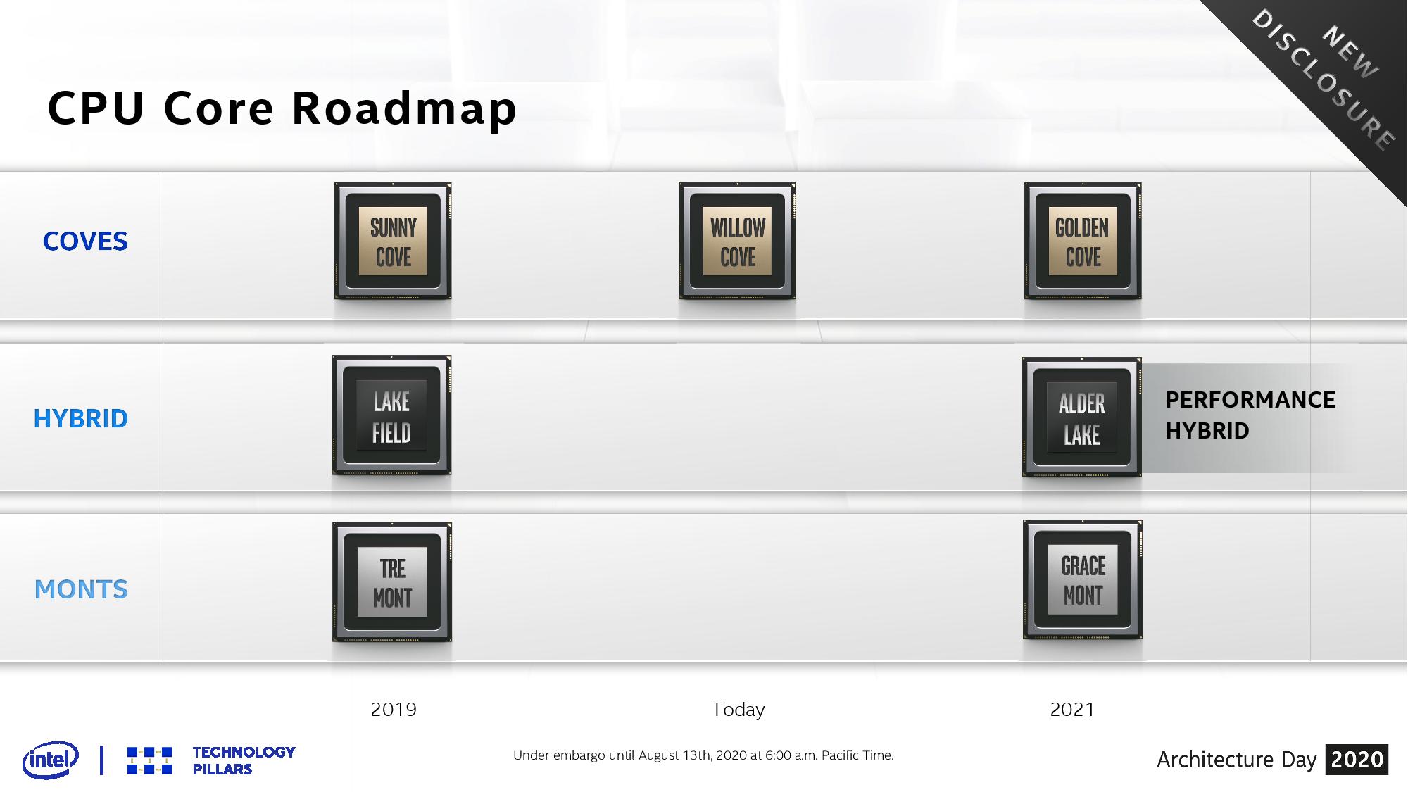
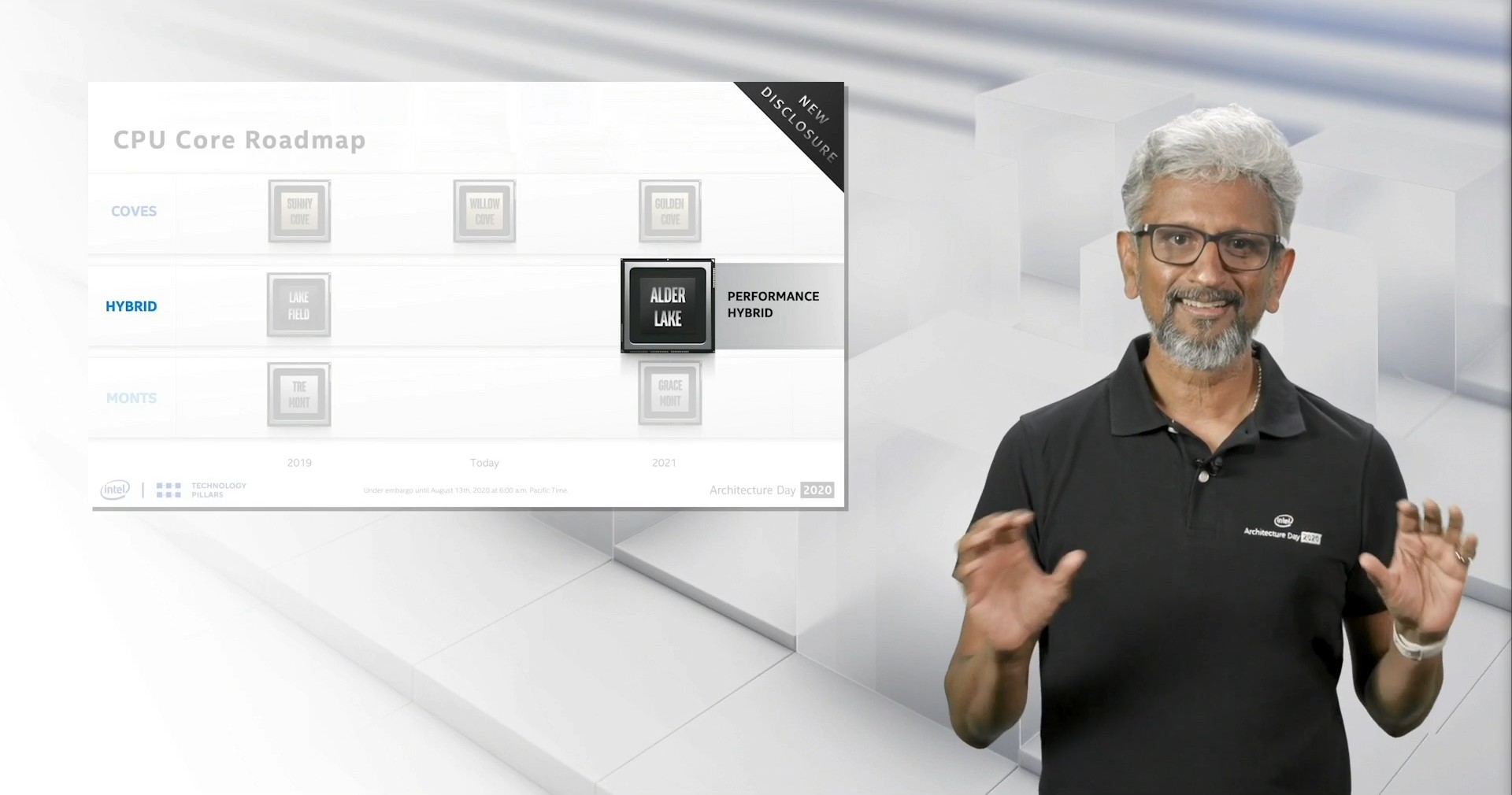
In the roadmap and as part of the discussions, Intel’s Raja Koduri confirms that Alder Lake will be a combination of the Golden Cove high performance computing core and the Gracemont high efficiency core, and the goal of this chip is to offer a ‘Performance Hybrid’ option into the portfolio. Raja explained to the audience that the company has learned a lot due to building Lakefield, its current hybrid x86 chip for thin and light notebooks, and while Lakefield was focused on battery life, Alder Lake will focus instead on performance.
Alder Lake will involve Intel’s next generation hardware scheduler, which we are told will be able to leverage all cores for performance and make it seamless to any software package. Intel claims that Alder Lake will be Intel’s best (ever? 2021?) performance-per-watt processor.
If leaks are to be believed, then Alder Lake looks set to offer an 8+8 design, although that has not been confirmed. Intel did not go into detail if Alder Lake will involve any next generation packaging, such as Foveros (which Lakefield does) – but in the Q2 2020 financial disclosures, it was said to be positioned for mobile and desktops. We expect Intel to discuss Golden Cove and Gracemont at some point next year, and then Alder Lake as an extension to those – we have already seen Intel documents regarding new instructions for each of these cores. My prediction is to come back this time next year, where we should have more to talk about.
Related Reading
- Intel Updates ISA Manual: New Instructions for Alder Lake, also BF16 for Sapphire Rapids
- Intel Roadmap Update: Alder Lake In H2’21, Ice Lake-SP Late This Year
- Intel’s 11th Gen Core Tiger Lake SoC Detailed: SuperFin, Willow Cove and Xe-LP
- The Intel Xe-LP GPU Architecture Deep Dive: Building Up The Next Generation
- The Intel Lakefield Deep Dive: Everything To Know About the First x86 Hybrid CPU


89 Comments
View All Comments
Meteor2 - Tuesday, August 18, 2020 - link
It's not low-end for its power and thermal envelopeseddman - Friday, August 14, 2020 - link
No 12 and 16 big core configs? Is this the only replacement for rocket lake, or they will have a non-hybrid line too?IINM Alder lake will be based on the golden cove arch, which allegedly is going to have a much higher IPC compared to skylake arch.
If so, does this mean intel is planning to counter AMD's core count with their big-little setup? I don't know what to think of this.
eddman - Friday, August 14, 2020 - link
Can we have an edit button already please? I re-wrote the comment a few times. At first I wanted to write "IINM Alder lake is going to have a much higher IPC".nandnandnand - Friday, August 14, 2020 - link
It's not too bad. Most games and applications won't use more than 8 cores, so there's a nice cluster of 8 Golden Cove performance cores in Alder Lake. The Gracemont cores are supposed to be near Ivy Bridge's IPC, although I guess they won't hit the same clocks.It would have been nice to see more small cores. Like 8+16 or 8+32 instead of 8+8. Oh well.
yeeeeman - Saturday, August 15, 2020 - link
I am guessing 10nm process is the limit here...nandnandnand - Saturday, August 15, 2020 - link
Is it going to be monolithic or chiplets though?https://www.tomshardware.com/news/intel-alder-lake...
"The smaller footprint on Lakefield enabled smaller, thinner, and lighter mobile designs by shrinking the size of the chip package with 3D stacking, but Intel doesn't have the same footprint concerns on the desktop. As such, Intel wouldn't necessarily have to use the cost-increasing Foveros 3D packaging technique to bring the processors to market. Instead, the chipmaker could use a single monolithic die with two kinds of cores, a chiplet-based architecture composed of separate compute chiplets for each type of core, or stick with 3D Foveros packaging. Only time will tell."
KimGitz - Sunday, August 16, 2020 - link
What would be the use case of having 32 or 16 Ivy Bridge type of Cores with 8 Golden Cove cores? On a desktop I would rather have 16 or 32 Golden Cove core instead of a Hybrid. On a Laptop you are constrained by the battery and thermals of the chasis. Seems like 4 Little core are 1 big core, that is what I think Intel was hoping with Lakefield. Once you go past 8 little cores it better to exchange a set of 4 little cores with 1 big core, for example instead of 6+12 it is better to exchange little cores and end up with 8+4. The big core are high performance Cores so once you need more performance they will always be better, if you need efficiency then what you need is not more Cores but how to do more with less. This is the philosophy being the bigLITTLE architecture. Once the performamce demand increases by due to multi tasking or high performance tasks it is no longer efficient to use the LITTLE core. Even with ARM SOCs we have performance increased by adding a better big core, for example Snapdragon 865 plus adds a prime core on top of the big Cores to get an edge on performance over the snapdragon 865. I could be very wrong in my analysis. So we will see how things pan out. I believe without the problems with 7nm and 10nm Intel would have used a chip let design for their desktop and a hybrid design for mobile. Intel struggled to get their chip let designs working even on the Xe-HP GPUs. AMD is really nailing it with their Infinity fabric and architecture.nandnandnand - Sunday, August 16, 2020 - link
It's a cheap way to get lots of multi-threaded performance. Less die area, less cost.The big core cluster can get loaded up with the tasks that need high single-threaded performance. Anything that is embarrassingly parallel could use dozens if not hundreds of small cores.
A hypothetical 8+32 configuration would have 8 big cores which could handle the most demanding threads, and would match the next-gen console core count by itself, meaning most gaming is covered for several years. Then the small cores can handle any background tasks and any software capable of using as many cores as you throw at it.
My understanding is that 1 big core is around the same die area as 4 small cores, but the small cores have more than 25% the performance of a big core. Maybe 50%? So 8+32 would have more total multi-threaded performance than 16 big cores, at around the same die area. 8+32 can credibly compete with AMD's 16-core, 8+8... not so much.
KimGitz - Monday, August 17, 2020 - link
Consider the performance of 8+32 vs 12+16 vs 16+0 (big+LITTLE), how will they rank?If we look at what is happening with smartphone SOCs which have more thermal constraints than laptops and desktops, for example the Snapdragon 600 series vs Snapdragon 700 series vs the 800 series vs Snapdragon 8cx performance is scaled up generation on generation by increasing and improving the big cores. The little cores have remained the same (Cortex A55) for several generations.
nandnandnand - Monday, August 17, 2020 - link
I remember seeing some disappointment over there being no Cortex-A55 successor, but has anybody provided an official explanation why that is?Intel has continued to improve its Atom line. Goldmont Plus (e.g. J4115) is being dumped into x86 single board computers right now, Tremont is in Lakefield, and Gracemont will be in Alder Lake.