Intel Xe-HP Graphics: Early Samples Offer 42+ TFLOPs of FP32 Performance
by Dr. Ian Cutress on August 21, 2020 11:00 AM EST- Posted in
- GPUs
- Intel
- Enterprise
- Intel Arch Day 2020
- XeHP

One of the promises that Intel has made with its new Xe GPU family is that in its various forms it will cater to uses ranging from integrated graphics all the way up to the high performance compute models needed for super-dense supercomputers. This means support for the types of calculations involved in simple graphics, complex graphics, ray tracing, AI inference, AI training, and the compute that goes into molecular modelling, oil-and-gas, nuclear reactors, rockets, nuclear rockets, and all the other big questions where more compute offers more capabilities. Sitting near the top of Intel’s offerings is the Xe-HP architecture, designed to offer high performance GPUs for standard server and enterprise deployments.

Over the past couple of weeks Intel has offered some of the first technical details of Xe-HP, following Raja Koduri showing it off across his social media profiles. We know that it is designed to be a modular architecture, with different chiplets connected together using Intel’s Embedded Multi-Die Interconnect Bridge technology. We also know, due to disclosures made at Intel’s Architecture Day, that it is set to be built on Intel’s 10nm Enhanced SuperFin (10ESF, formerly 10++, formerly 10+++) manufacturing process, which we believe to be a late 2021 process. Raja Koduri promised during the Architecture Day presentation that Xe-HP (and Xe-HPG) will be available in 2021.

Intel explained that the modular Xe-HP design will scale from one to four tiles, and the concept of Xe-HP was to ‘scale everything’, such as execution units, frequency, bandwidth, IPC, and math capabilities. We assume that each tile will have direct access to some on-chip memory as well – truly scaling up every aspect of a chip – although how the chip's HBM2E is allocated hasn't been confirmed. The point of the product is that it is designed for the data-center, so there needs to be a mix of media compute as well as raw compute, covering all sorts of uses cases.

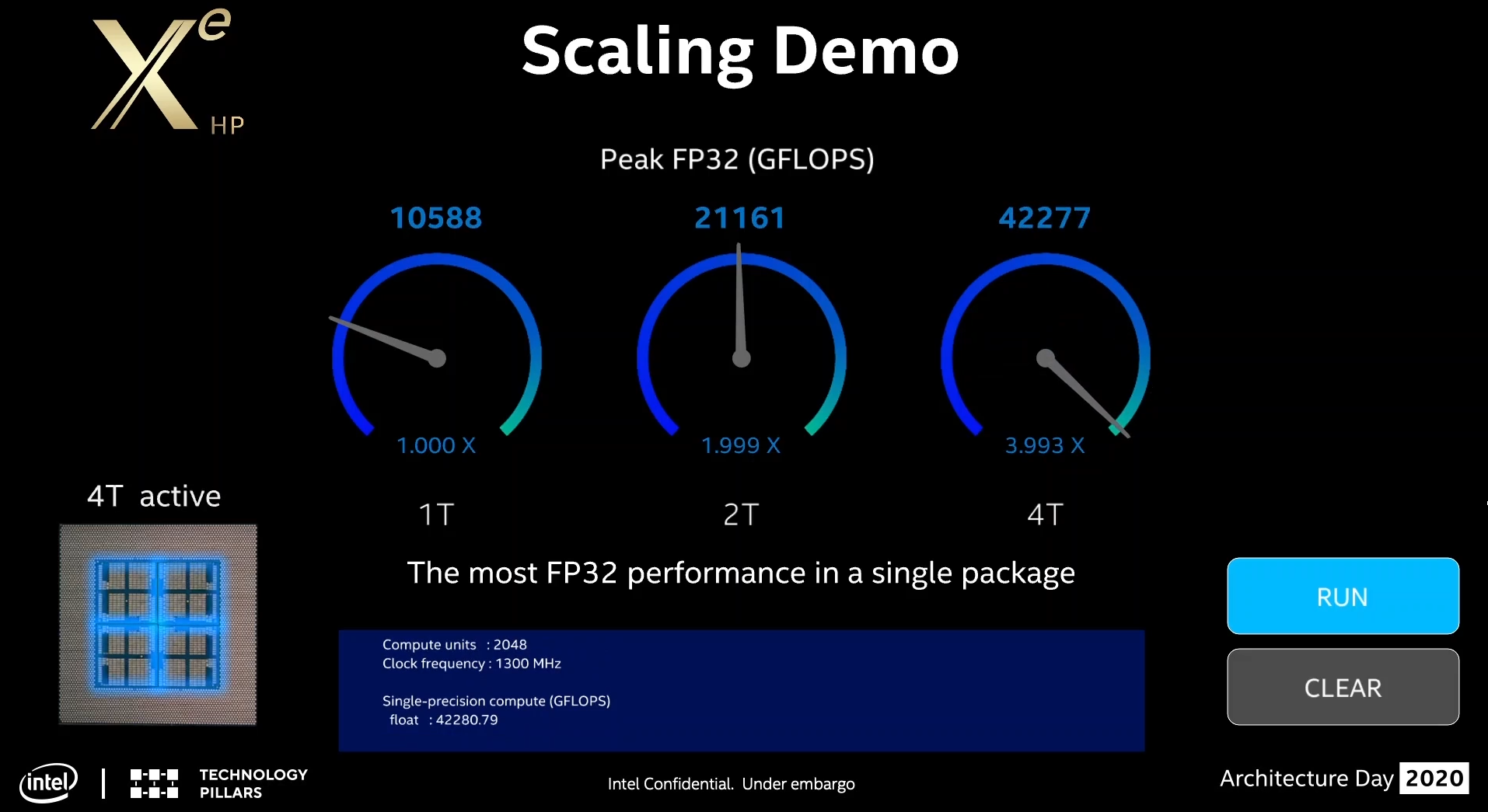
As part of the demonstration during Architecture Day, Intel also showcased that they’ve been running some benchmarks on the early silicon in the labs. By early silicon, we mean that these aren’t running at the final frequencies, this isn’t final firmware, and the software stack still has a way to go, so undoubtedly there are optimizations at every level.
First, Intel showed that a single tile of Xe-HP can not only transcode one 4K60 video in real time, but ten. In the demonstration they had the FFmpeg output, showing that the demo was converting each video from 5332 kb/s overall down to 3000 kb/s average (6000 kb/s max).
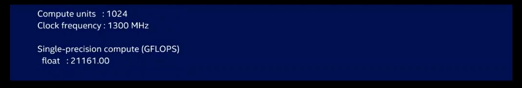
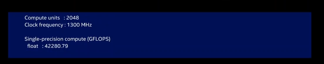
For compute, Intel offered the following performance numbers, given as peak GFLOPs of FP32 math using the OpenCL-based CLPeak benchmark.
- One Tile: 10588 GFLOPs (10.6 TF) of FP32
- Two Tile: 21161 GFLOPs (21.2 TF) of FP32 (1.999x)
- Four Tile: 42277 GFLOPs (42.3 TF) of FP32 (3.993x)
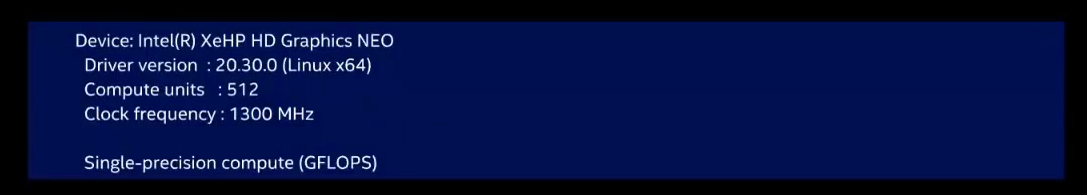
We also get some additional information from the video of Xe-HP. The tests were done on Linux, and actually all done on a version of the quad-tile chip, but made to run in 1T/2T/4T modes. This is why when looking at the video we can see all three versions are running at 1300 MHz. The string used for the chip is ‘XeHP HD Graphics NEO’ as well.
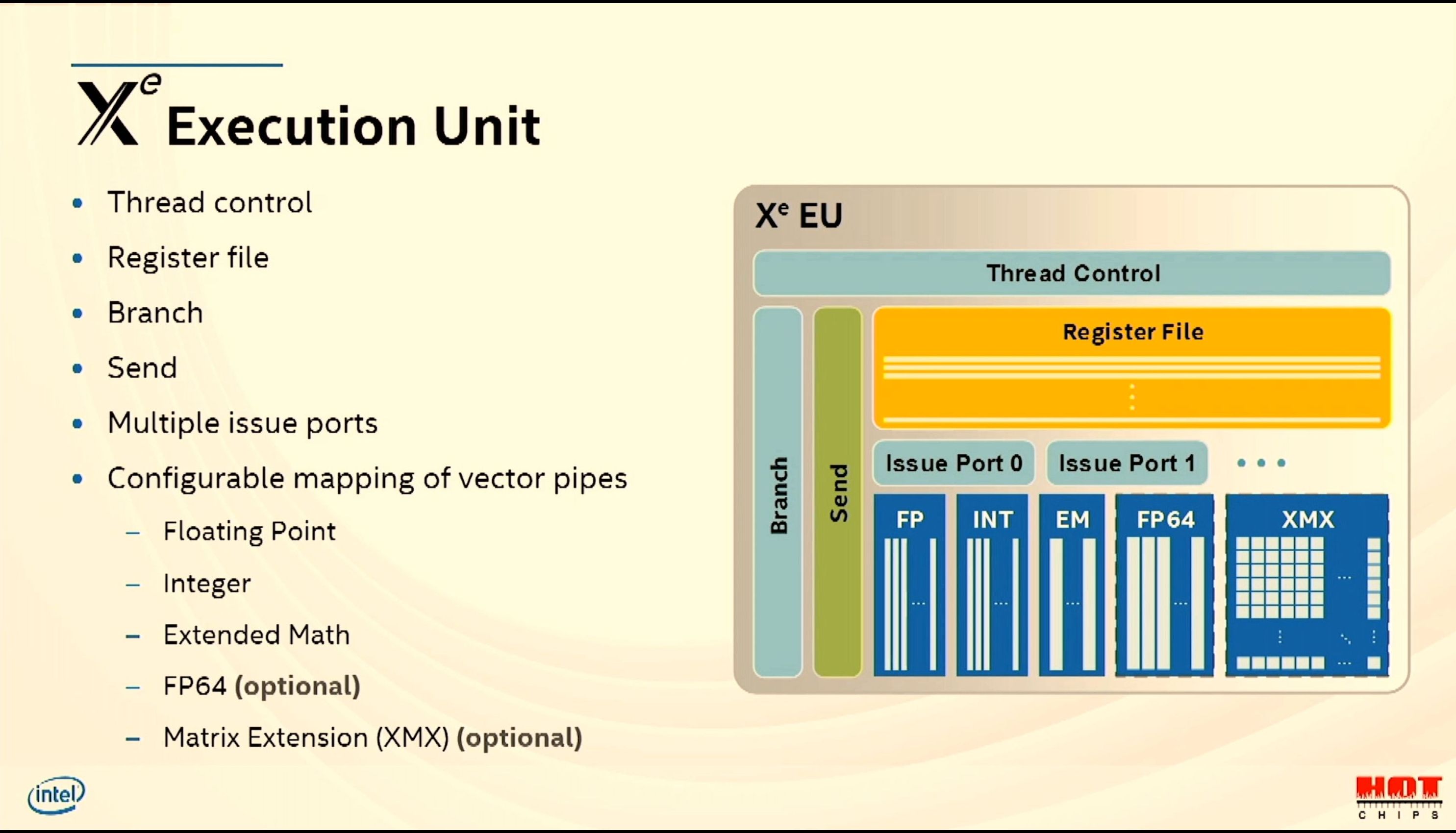
The video also shows that a single tile has 512 ‘compute units’, while the dual tile has 1024 compute units and the quad-tile has 2048 compute units. And while Intel hasn't officially claried what "compute units" mean in this context, the performance figures all but confirm that it's counting Intel's Execution Units. Based on the given GFLOPs, the stated clock speed, and the Xe architecture's 8 pipes per Execution unit with dual FMAs, Intel's performance figures map to 512/1024/2048 EUs respectively. That would mean that each one would have:
- One Tile: 512 EUs = 4096 ALUs (+ 1024 Extended Math ALUs)
- Two Tile: 1024 EUs = 8196 ALUs (+ 2048 Extended Math ALUs)
- Four Tiles: 2048 EUs = 16384 ALUs (+ 4096 Extended Math ALUs)
This is assuming that the Execution Unit structure of 8+2 from Xe-LP remains. We know that HP will support new XMX instructions for matrix math, as well as AI-related quantization levels and FP64 too. Which Intel's Hot Chips presentation has confirmed will be implemented within the EUs as additional physical blocks.
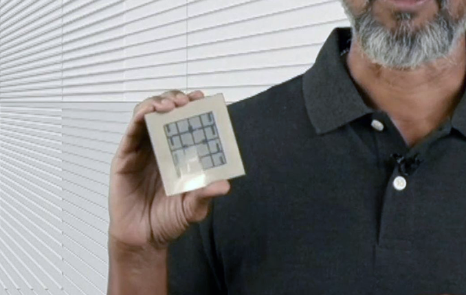
There was also a shot of the rear of an Xe-HP die, which Raja has shown off during his Hot Chips keynote as well. We can play a game of count the pins.
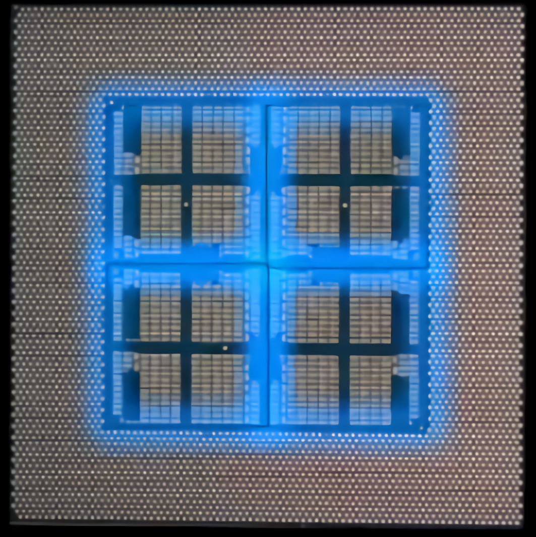
Intel Xe-HP 4-Tile Rear
Intel believes it is achieving near linear scaling in compute performance across its multi-tile strategy – at least up to 4T using CLPeak, a benchmark designed to measure a GPU's maximum compute throughput. There’s nothing here to say about tile-to-tile bandwidth scaling, or if this multi-tiling strategy and NUMA arrangement of tiles has knock-on effects for memory-limited or sparse math – Intel’s goal was simply to show that the hardware is running and what kind of peak compute performance it can offer. There’s also no word on power consumption either, or cost, however in the presentation Intel says that the goal here is to offer the equivalent of a rack-scale transcoding system in a single chip with best-in-class TCO, winning on performance-per-watt-per-dollar.
Xe-HP is set to be available in 2021 for the Enterprise market.
Related Reading
- The Intel Xe-LP GPU Architecture Deep Dive: Building Up The Next Generation
- Intel’s Xe-HPG GPU Unveiled: Built for Enthusiast Gamers, Built at a Third-Party Fab
- Intel Xe-HPC GPU Status Update: 4 Process Nodes Make 1 Accelerator
- Spotted At Hot Chips: Quad Tile Intel Xe-HP GPU
- Hot Chips 2020 Live Blog: Intel's Xe GPU Architecture (5:30pm PT)


41 Comments
View All Comments
Santoval - Friday, August 21, 2020 - link
Perhaps you are a shill for both, they are not necessarily mutually exclusive :p/s
Slash3 - Friday, August 21, 2020 - link
I appreciate the coverage, regardless of which company a given event may feature.Spunjji - Monday, August 24, 2020 - link
Some people will always get upset not just at the level of obfuscation in a company's marketing - which is sometimes fair - but at the sites that relay it, which is just bizarre. How else are we supposed to have a laugh at the desperation if we don't get to see it? 😬Solidstate20 - Wednesday, August 26, 2020 - link
I've never created an account since I never felt the need to post a comment. I created one just now because I just wanted to say Ian that for every Internet Troll posting that you are "a shill" there are a hundred of us quiet readers who enjoy your news coverage, the quality, depth and insight. Keep doing it and don't feel the need to feed the trolls :)HardwareHut - Friday, August 21, 2020 - link
Those numbers (42.3 TF of FP3) of the Xe-HP is with matrix math instructions.The A100 peaks at 156 TF of FP32 with tensor cores, and at 312 TF of FP32 with sparsity.
The 19.5 TF of FP32 that you are citing for the A100 is of FMA only - no tensor cores (matrix math).
Ian Cutress - Saturday, August 22, 2020 - link
These Intel numbers are through the ALUs, not XMX.p1esk - Saturday, August 22, 2020 - link
Tensor cores are FP16 multipliers with FP32 accumulators. Apples to oranges.CiccioB - Tuesday, August 25, 2020 - link
With Ampere the tensor cores are now FP32, not FP16.And can also do FP64 math, at a reduced speed.
Spunjji - Monday, August 24, 2020 - link
I don't in the least agree that Anandtech are a "247 shill for intel". They're definitely passing the figures on with a degree of enthusiasm intact, but at no point did I feel like this was different from how they treat any other company's products.What is clear is that Intel are engaging in a broad-spectrum marketing onslaught with a bunch of un-launched products right now. They're allowed to do that, and you're allowed to add whatever dose of seasoning you find appropriate.
JayNor - Monday, August 24, 2020 - link
Raja said the Xe-HP products go up to 300W range. However, that was back in Dec, 2019.https://youtu.be/-kWiRrf2o6Q?t=2156