Intel Moving to Chiplets: ‘Client 2.0’ for 7nm
by Dr. Ian Cutress on August 21, 2020 5:00 PM EST- Posted in
- CPUs
- Intel
- GPUs
- Client
- Intel Arch Day 2020
- Client 2.0
One of the more esoteric elements of Intel’s Architecture Day 2020 came very near the end, where Intel spent a few minutes discussing what it believes is the future of some of its products. Brijesh Tripathi, VP and CTO of Intel’s Client Computing group, laid out a vision about the future of its client products in the 2024+ future timeframe. Centered around Intel’s 7+ manufacturing process, the goal was to enable ‘Client 2.0’ – a new way to deliver and enable immersive experiences through a more optimized silicon development strategy.
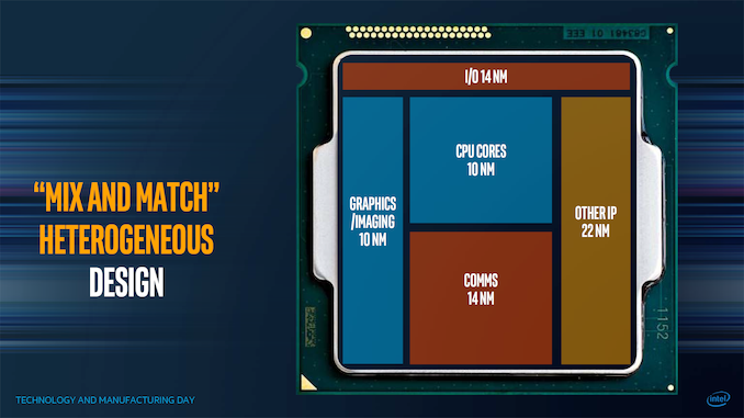
Chiplets aren’t new, especially with recent launches from Intel’s competitors, and as we move into more complex process node development, the era of chiplets enables faster time-to-market as well as better binning and yields for a given product. The key is enabling how those chiplets fit together, and at which points it makes sense to mix and match the relevant ones. Intel has spoken about this before in a more generalized context, at its Technology and Manufacturing Day 2017, as shown in the carousel image at the top.
The goal here is to mix and match which process nodes work best for different parts of the chip. Intel seems set to realize this vision starting with its 7nm platform. At Architecture Day 2020, Brijesh Tripathi showed this slide:
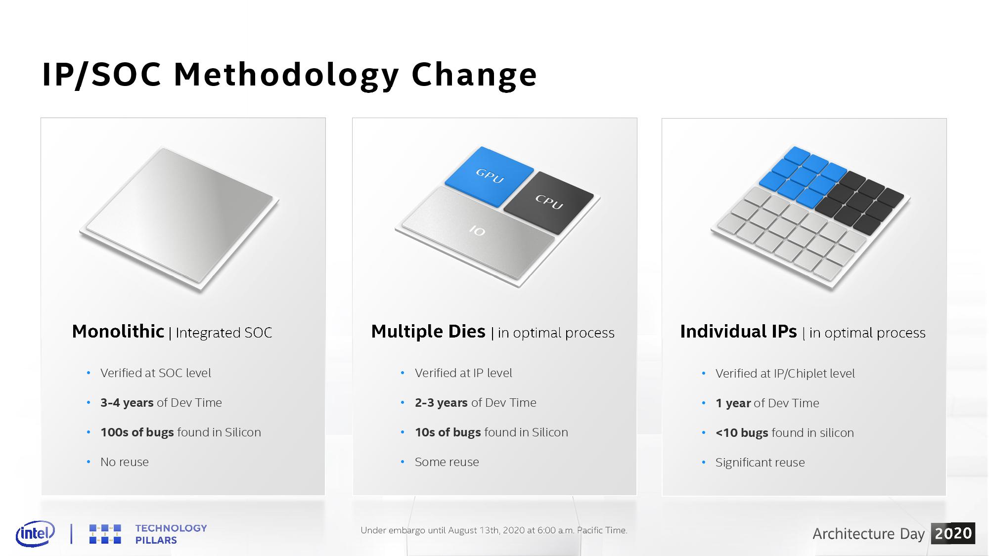
On the left is a typical chip design – monolithic with everything it requires. For Intel’s leading edge products, these take 3-4 years to develop, and bugs are found in silicon by both Intel initially and then later by Intel’s partners as they can ramp up the silicon-on time by a a few orders of magnitude.
In the middle is a basic chiplet layout, similar to that slide from 2017, where different functions of the die are split into their own modules. Assuming a consistent interconnect, there are some reuse of the silicon elements, such as AMD using the same core compute dies in client and server. For some semiconductor companies (except Intel), this is where we are.
On the right is where Intel sees its future. Instead of having a single digit number of chiplets in a product, it envisions a world where each IP can be split into multiple chiplets, enabling products to be built with different configurations of what works for the market. In this instance, a chiplet might be a PCIe 4.0 x16 link – if the product needs more, it simply adds in more of these chiplets. Same with memory channels, cores, media accelerators, AI accelerators, Ray Tracing engines, crypto accelerators, graphics, or even as far down as SRAM and caching blocks. The idea is that each IP can be split and then scaled. This means that the chiplets are tiny, can be built relatively quickly, and bugs should be ironed out very quickly.

In this diagram, we are treated to Intel’s long term vision for the client – a base interposer with an in-package memory (something like an L3 or L4) that can act as the main SRAM cache for the whole die, and then on top of this we get 24 different chiplets. Chiplets can be graphics, cores, AI, Media, IO, or anything else, but they can be mixed and matched based on what is needed. A content creator might want a balance between some good graphics acceleration and compute, while a gamer might want to focus purely on the graphics. A corporate client or workstation might need less graphics and more for compute and AI, whereas a mobile version of the chip will be heavily invested in IO.
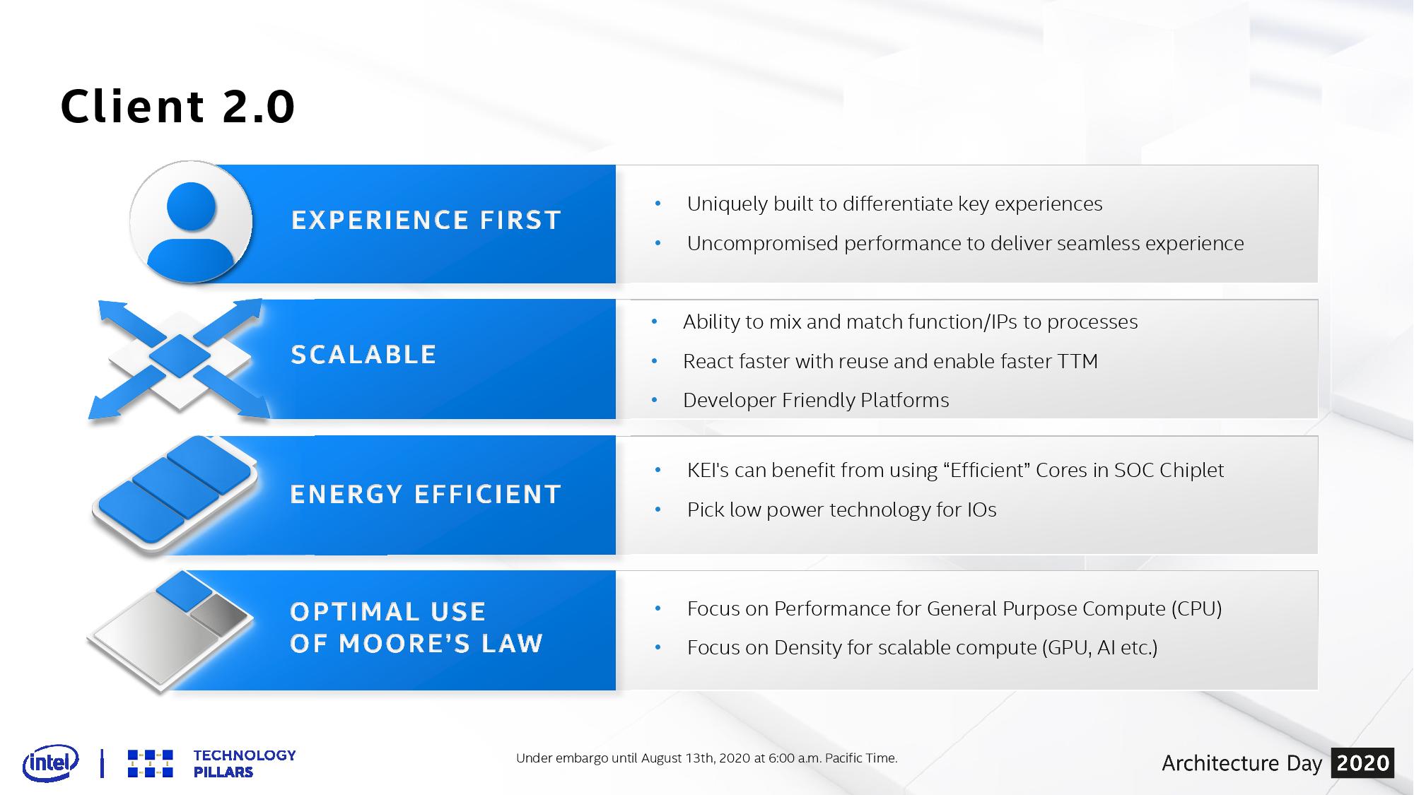
As always, there is some trade-off between chiplet size and complexity of actually putting them together in a multi-die arrangement. Any communications between chiplets costs more power than a monolithic interpretation, and usually offer higher latency. Thermals have to be managed as well, and so sometimes those chiplets are limited by what thermal properties are available. Multi-die arrangements also cause headaches for mobile devices, where z-height is critical. However, the benefits afforded from using the right process at the right time for the right product are big, as it helps provide both performance and power at the best possible cost. It also gives the opportunity to bring in 3rd party IP quickly if something amazing hits the scene.
The only downside here is that Intel hasn’t spoken much about the glue that binds it all together. Chiplet strategies rely on complex high-speed interconnect protocols, custom or otherwise. Current uses of Intel’s die-to-die connectivity are either simply memory protocols or FPGA fabric extensions – the big ones for server CPUs like UPI aren’t necessarily up to the task. CXL could be the future here, however current CXL is built upon PCIe, which means a complex CXL/PCIe controller for every chiplet which will likely get power hungry fast.
Intel has stated that they are inventing new packaging technology and new levels of connectivity to act between the silicon - there is no disclosure on the protocols at this time, however Intel acknowledges that to get to this level of scale it will have to go beyond what the company has today, and that will require creating standards and innovation in this area. The goal is to create and support standards, and the first incarnation will have some standardization built in. Intel states that this is a method of extreme disaggregation, and to note that not everything that is connected has to be high bandwidth (such as USB) or a coherent interconnect - Intel sees the goal involving a handful of protocols throughout the spectrum.
There’s also the developer market, which might be used to a more homogeneous implementation of resources in any given product. Without careful planning, and relevant coding, there is the potential for certain chiplet configurations to fall over if the developer was expecting a certain ratio of compute to graphics, for example. This isn’t something that OneAPI could easily fix.
These are all issues that Intel will have to address, although they have a few years until this comes to fruition. We were told that the internal name is Client 2.0, although it will likely have more marketing dressing added as Intel starts talking about it in more detail.
Related Reading
- Intel's Interconnected Future: Combining Chiplets, EMIB, and Foveros
- Intel 7nm Delayed By 6 Months; Company to Take “Pragmatic” Approach in Using Third-Party Fabs
- The Intel Lakefield Deep Dive: Everything To Know About the First x86 Hybrid CPU
- Intel to use Nanowire/Nanoribbon Transistors in Volume ‘in Five Years’


67 Comments
View All Comments
yetanotherhuman - Monday, August 24, 2020 - link
Now with special Intel Glue-Not-Glue™londiste - Monday, August 24, 2020 - link
I think most of the failure in what you are describing is about process node and failure to manufacture and bring new stuff to market en masse.Architecturally speaking - especially of core, iGPU - while Skylake-derived Comet Lake is still what we get on the desktop Intel has Ice Lake with Sunny Cove and Gen11 iGPUs since last year. Tiger Lake with more improvements is expected early next year, if I remember correctly.
Zen and Zen+ had shortcomings compared to Skylake-ish and while Zen2 had a nice jump in terms of "IPC" (technically single-core performance at iso-frequency) Ice Lake and Sunny Cove have proven to be a bit above that but let down by Intel's failing 10nm process.
Upcoming Zen3 and Tiger Lake might be closer than we are assuming them to be. Unless something has changed considerably, we as out of luck on the desktop with Intel unable to compete but again - when it comes to architecture Intel really is not behind or not that far behind.
ARM is nice but I would not draw too many conclusions from current news about fast improvements. ARM is undoubtedly improving, growing larger and faster but majority of the changes that are made follow the same path more mature performance/oriented ISAs (like x86) have gone through. ARM CPUs - or rather, SoCs - are also manufactured on bleeding edge nodes, even ahead of AMD and TSMCs cooperation. 5nm SoCs in phones will be out something like a year before Zen4 gets to the performance variation of the same node.
When it comes to competition and ARM encroaching on x86-s playground from the lower power angle, do not count out Intel or AMD. Tremont seems to be noticeable improvement on Atom line after years of neglect and that is probably not a coincidence. AMD definitely has capability to follow, Jaguars were OK and they can pick up where they left off. While performance of these pales in comparison to Lakes or Coves and Zens they are also much smaller and much more efficient. Even Intel is apparently able to manufacture Tremont-based SoCs reasonably well on the 10nm node.
JayNor - Tuesday, August 25, 2020 - link
Intel also confirmed a Tiger Lake-H recently with some linux patches. The recent presentations indicate Tiger Lake's 10nm SuperFin transistors should do well out to 65W.Recent leaks indicate Intel will also build a 14nm Rocket Lake-S with PCIE4.
edzieba - Monday, August 24, 2020 - link
"The only downside here is that Intel hasn’t spoken much about the glue that binds it all together"Ian, you yourself blogged about the interface three years ago! https://www.anandtech.com/show/11748/hot-chips-int...
It's the same AIB interface provided to the DARPA CHIPS initiative for implementation by other vendors: https://www.anandtech.com/show/13115/intel-provide...
Spunjji - Monday, August 24, 2020 - link
The "glue" being referred to there is the interconnect architecture - think of AMD's Infinity Fabric - rather than the physical method of bonding the things together, which is what EMIB does.They'll need to design a flexible interface through which these various components can communicate at the required speeds while using a minimum of power and area. Until they do that (and I don't doubt they're capable) none of this makes any sense as an actual product.
edzieba - Monday, August 24, 2020 - link
"They'll need to design a flexible interface through which these various components can communicate at the required speeds while using a minimum of power and area"Which is AIB (Advanced Interface Bus). Which is what the two articles I linked mentioned.
alufan - Monday, August 24, 2020 - link
Nice to see the sites virtually all Intel front page again apart from AMD B550 motherboard thats been there for several Days there must be at least 10 articles about Intel and its products on the front page