What Products Use Intel 10nm? SuperFin and 10++ Demystified
by Dr. Ian Cutress on September 25, 2020 9:00 AM EST_678x452.jpg)
For our audience that regularly keeps track of Intel’s product portfolio, it would be hard to miss that the naming strategy of Intel’s process node technologies is a bit of a mess. To some, those words are themselves an understatement, as Intel has shifted its naming strategy 2-3 times since the launch of Intel’s first 10nm products. Not only that, even Intel’s various departments internally have a hard time keeping track of ‘what is this manufacturing process being called today’ when the press like AnandTech ask for details on the latest upcoming products.
Knowing this, and knowing what issues Intel has been having, I wanted to demystify Intel’s manufacturing process naming scheme such that users and engineers alike, even if they are inside Intel, can understand what is what but also importantly why. The why is the crucial factor.
If you're looking for a handy decoder ring for Intel's 10nm Products, it's here in page 3.
Why Do We Have Multiple Versions of a Process?
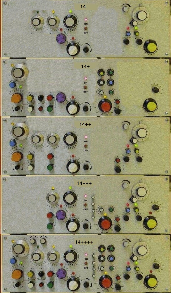
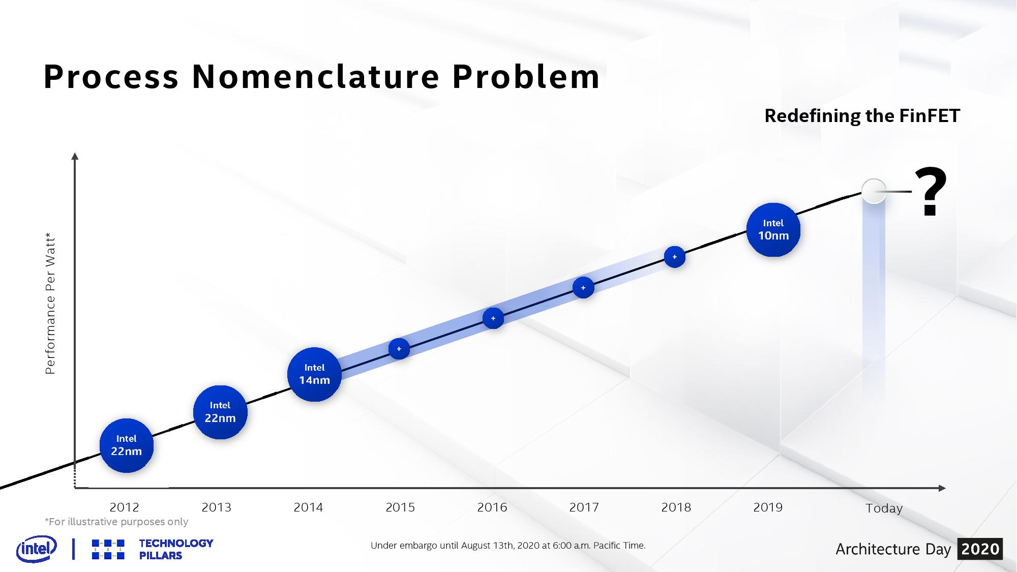
With Intel’s 14nm, we were invited to 14nm, 14+, 14++, 14+++, and if you believe Intel’s own slides, there were variants that went beyond this ++++ naming scheme. Each one of those additional + points on the end of the name signified a change in the process technology – usually to assist for increasing performance or efficiency.
Each one of these + points is an update to the BKM, or Best Known Methods.
While an engineer can draw an electrical layouts for a part of a processor, such as an addition circuit, actually applying that design to a silicon floorplan for manufacturing is a different skill altogether. Transistor libraries are designed to take advantage of a given process, and when a floorplan is optimized for a process, it can then be pasted and repeated as necessary – on top of this, simulation on thermals, power, and current density are applied to ensure that there are no hotspots or that critical paths inside the design have as few bottlenecks as possible.
When an update to the BKM occurs, two things can happen. Normally we see the update on the level of the transistor library that is changed – if the distance between two fins on a transistor increases for example, the transistor library and the macros may be made bigger, and then the floorplan might be redesigned to take account for this. As for any process node design, there are 100 different controls, and improving one might make three other controls worse, so it is a fine balancing act. Not only this, but the BKM has to be validated at the manufacturing level. The BKM update could apply to the metal stack as well, which in of itself can adjust the performance.
Lots of dials at each stage
In the long long past, BKM updates were never advertised externally. If Intel or TSMC or another foundry discovered a way to improve the performance, or decrease the voltage, or improve the yield, the update was silently rolled into the design and nothing much was made of it. Sometimes processors would be listed as ‘1.0 volts to 1.35 volts’, and it would just be a roll of the dice if a user obtained one of the lower voltage models.
However, as time between different process node updates has elongated, these BKM updates have started to be identified and effectively monetized by the semiconductor companies. An update to a process that improves the voltage by 50 millivolts and increases frequency by 200 MHz immediately becomes a productizable event, and products built on these updates can be offered for more money over the usual. Or, depending on the rate of updates, the whole next generation of products could be built on the update.

So we never saw BKM updates officially announced at Intel’s 45nm, 32nm, or 22nm process nodes. These updates were fast enough that the productization of any update didn’t warrant a full round of marketing. With 14nm, that changed.
Intel had discussed its roadmap beyond 14nm since its 2010 Investor Meeting. It predicted that the company would be on 14nm by 2013, 10nm by 2015, and 7nm by 2017. As we now know, 14nm was two years late, and 10nm was 2-4 years late. Because of the introduction of 10nm being delayed, Intel decided to productize its 14nm BKM updates, and signified those with + points.
Intel’s current official line is that there have been four updates to 14nm, creating five ‘generations’.
More Plus Means More Meme
Because of all the + points, Intel’s marketing sometimes getting it wrong, and perhaps a little bit of ‘++’ in most programming languages meaning ‘+1’, the whole concept of adding + to the process node has become a meme – a meme at Intel’s expense, purely on the basis of its failure to deliver 10nm before the 14++++ naming scheme got out of hand.


143 Comments
View All Comments
TheJian - Wednesday, September 30, 2020 - link
They did that to sell old chips stuck in inventory forever; nintendo probably got a great deal on stuff that at that at point was worth $0 to Nvidia. They didn't say whatever dude, they said no margin and robs from core R&D so we passed. The didn't pursue Nintendo, it's old crap that couldn't be sold to anyone else.NV doesn't do poor stuff until forced, or they simply have nothing else to sell more of, get it? If I've tapped out the entire gpu market, making a mint, etc, then make poor stuff if you still have resources. IE, if NV is short on silicon they put out low models LAST (heck they pretty much always do it, smarter).
What kind of soc is in that premium console from nintendo? Hint, it's not 7nm in that first one.
https://arstechnica.com/gaming/2016/12/nintendo-sw...
Hybrid consoles use "LAST GEN TECH". So they didn't waste tons of R&D did they? :) They are also very small chips even with the new ones (the lite model has newer tech, old T4 was ~100mm^2). Xbox/ps4 were 400+. Those puny ones won't steal much from the 3000's right? They went to samsung, so this deal might have been all they could get out of TSMC at the time (apple was buying all 7nm, now moved to 5nm, amd/intel bought a bunch of the freed up stuff).
Selling your own console and a chip in others for $10-15ea is very different, and also brought their store for game sales (income off other's work). Not the same as 450mm^2 console chips for $10-15 each when those could be flagship cpu/gpus that make $100 or more. NV just ran out of cards in minutes. AMD claiming they won't. It would be a lot easier if you weren't wasting silicon on $15 items right? That size is a large AMD gpu not being sold for $500+. IE, 3070 is ~393mm^2. NV makes more than $15 on them. As the poor guy in semi, you should concentrate on INCOME, not units or share. This has nothing to do with being cool, it wasting R&D. It's about money, so yeah, legit. Your comment? Stupid. Intel screwed the lowend when short 10% silicon (couldn't fill about 10% of customers PC's), and moved to HEDT/server. You don't seem to understand the conversation or how these companies work.
Shield was an attempt again, to move old silicon and only cost 10mil to dev both shield TV and the handheld they said...That is a small price to pay to move old chips worth at least as much and collect some money on the store maybe, push streaming, etc etc. It was a small price to pay and a good move business wise at the time. They failed in mobile so tried to recover some of the wasted silicon collecting dust and push new streams of income while doing it. Good management. These end up in AMD writeoffs (see trinity etc IIRC, multiple apu junk).
They are no xbox/sony because they wanted MORE money. You are proving my point. AMD sold out cheap, NV wouldn't. Yeah, you're right. Thanks. They tried to MAKE MONEY, not RIP off MSFT. I wouldn't work for free either basically. :) 15%, in semi? ROFL. Only if I can't make more on something else ANYWHERE. Note xbox360 cost MSFT 3.5B or so, and Sony's lost ~4B...ROFL. Jury still out on ps4/xbox1 etc. AMD thought they might beat NV tech by being in a console and hoping games would aim at them, fixing their perf problems vs. NV gpus. It's not working. See 9% going to NV over TECH. RT+DLSS sells...OUT that is..In minutes.
Wake me when you actually have a data point and learn to debate. See Paul Graham's chart.
Teckk - Wednesday, September 30, 2020 - link
Yes, all fabs at full steam. Funny you forgot about 10nm and 7nm."but it is only until they right the fab ship and they have many ways to do that." like they've been doing it for last 4 SkyLakes? Or was it 5? You're good at counting you will know that for sure.
Come for a bebate when you actually know something about the process nodes and where they are. Play with historical numbers till then. That's what they are. Historical.
Tilmitt - Sunday, September 27, 2020 - link
Is Anandtech aware that Nvidia Corporation has released a new series of 3D accelerator boards?Qasar - Monday, September 28, 2020 - link
they are, but there are these fires in California.......Sychonut - Monday, September 28, 2020 - link
Excessive politics + power hungry Murthy = delaysdeil - Monday, September 28, 2020 - link
I am not sure how reliable that source is, but I heard Intel could not get double-digit yields on 10nmat first, then after making design less "innovative", but yields were okaying, performance was within margin of error from 14nm+++++++++++++
Spunjji - Monday, September 28, 2020 - link
Entirely reliable.In practice, Ice Lake is roughly comparable to Comet Lake in everything but GPU performance; overall what it gained in IPC it lost in clock speed. This was *after* Intel had already relaxed their 10nm transistor density way below their initial claims of 67-100 million transistors per square millimetre.
They finally seem to have fixed that with Tiger Lake, but given the paper-launch nature of that release and their reluctance to discuss the 8-core variants, I'd be happy to surmise that either yields are still not great or they only have some fraction of their 10nm fab resources capable of manufacturing on the new "SuperFin" node variant.
RedOnlyFan - Saturday, October 3, 2020 - link
@spunjji Your delusional comments deserves a praise.Linustechtips12 - Monday, September 28, 2020 - link
Look honestly since intel didn't have completion why wouldn't you stay roughly on the same node it saves money and time somewhat you can argue that they should've been innovation but are people forgetting they own stock in amd toAgent Smith - Monday, September 28, 2020 - link
They're going to drown in those lakes