Apple Announces The Apple Silicon M1: Ditching x86 - What to Expect, Based on A14
by Andrei Frumusanu on November 10, 2020 3:00 PM EST- Posted in
- Apple
- Apple A14
- Apple Silicon
- Apple M1
Apple's Humongous CPU Microarchitecture
So how does Apple plan to compete with AMD and Intel in this market? Readers who have been following Apple’s silicon endeavors over the last few years will certainly not be surprised to see the performance that Apple proclaimed during the event.
The secret sauce lies in Apple’s in-house CPU microarchitecture. Apple’s long journey into custom CPU microarchitectures started off with the release of the Apple A6 back in 2012 in the iPhone 5. Even back then with their first-generation “Swift” design, the company had marked some impressive performance figures compared to the mobile competition.
The real shocker that really made waves through the industry was however Apple’s subsequent release of the Cyclone CPU microarchitecture in 2013’s Apple A7 SoC and iPhone 5S. Apple’s early adoption of the 64-bit Armv8 ISA shocked everybody, as the company was the first in the industry to implement the new instruction set architecture, but they beat even Arm’s own CPU teams by more than a year, as the Cortex-A57 (Arm own 64-bit microarchitecture design) would not see light of day until late 2014.
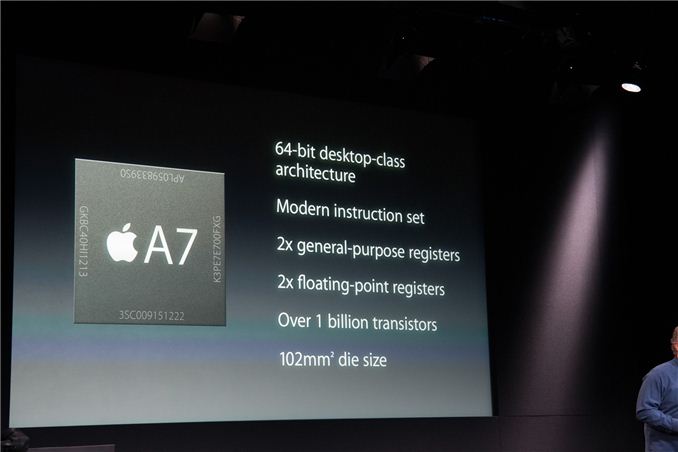
Apple famously called their “Cyclone” design a “desktop-class architecture” which in hindsight probably should have an obvious pointer to where the company was heading. Over subsequent generations, Apple had evolved their custom CPU microarchitecture at an astounding rate, posting massive performance gains with each generation, which we’ve covered extensively over the years:
| AnandTech A-Series Coverage and Testing | ||
| Year | Apple A# | Review / Coverage |
| 2012 | A6 | The iPhone 5 Review |
| 2013 | A7 | The iPhone 5s Review |
| 2014 | A8 | The iPhone 6 Review |
| 2015 | A9 | The Apple iPhone 6s and iPhone 6s Plus Review |
| 2016 | A10 | The iPhone 7 and iPhone 7 Plus Review |
| 2017 | A11 | - |
| 2018 | A12 | The iPhone XS & XS Max Review |
| 2019 | A13 | The Apple iPhone 11, 11 Pro & 11 Pro Max Review |
| 2020 | A14 | You're reading it |
This year’s A14 chip includes the 8th generation in Apple’s 64-bit microarchitecture family that had been started off with the A7 and the Cyclone design. Over the years, Apple’s design cadence seems to have settled down around major bi-generation microarchitecture updates starting with the A7 chipset, with the A9, A11, A13 all showcasing major increases of their design complexity and microarchitectural width and depth.
Apple’s CPUs still pretty much remain a black box design given that the company doesn’t disclose any details, and the only publicly available resources on the matter date back to LLVM patches in the A7 Cyclone era, which very much aren’t relevant anymore to today’s designs. While we don’t have the official means and information as to how Apple’s CPU work, that doesn’t mean we cannot figure out certain aspects of the design. Through our own in-house tests as well as third party microbenchmarks (A special credit due for @Veedrac’s microarchitecturometer test suite), we can however unveil some of the details of Apple’s designs. The following disclosures are estimated based on testing the behavior of the latest Apple A14 SoC inside of the iPhone 12 Pro:
Apple's Firestorm CPU Core: Even Bigger & Wider
Apple’s latest generation big core CPU design inside of the A14 is codenamed “Firestorm”, following up last year’s “Lightning” microarchitecture inside of the Apple A13. The new Firestorm core and its years long pedigree from continued generational improvements lies at the heart of today’s discussion, and is the key part as to how Apple is making the large jump away from Intel x86 designs to their own in-house SoCs.
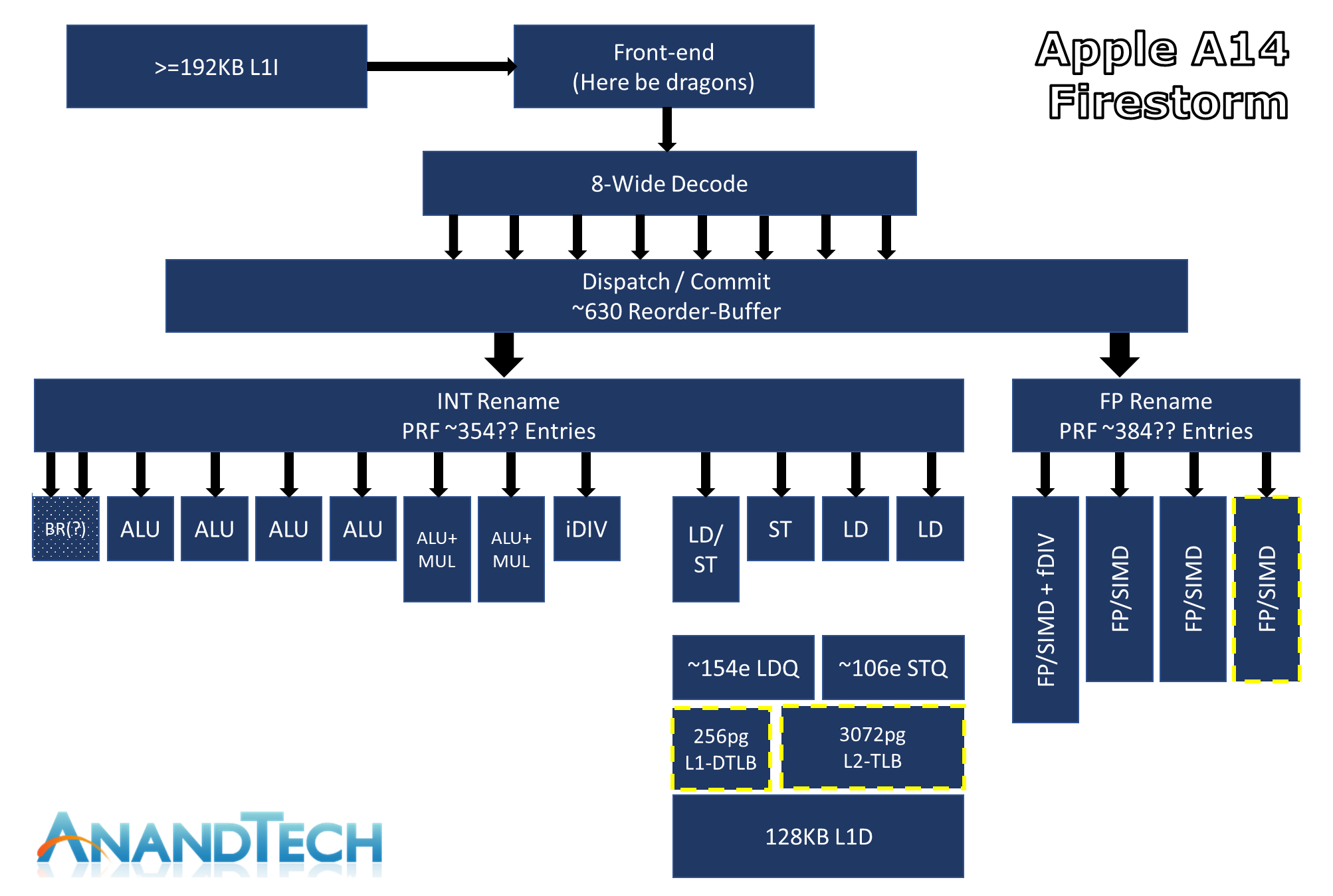
The above diagram is an estimated feature layout of Apple’s latest big core design – what’s represented here is my best effort attempt in identifying the new designs’ capabilities, but certainly is not an exhaustive drill-down into everything that Apple’s design has to offer – so naturally some inaccuracies might be present.
What really defines Apple’s Firestorm CPU core from other designs in the industry is just the sheer width of the microarchitecture. Featuring an 8-wide decode block, Apple’s Firestorm is by far the current widest commercialized design in the industry. IBM’s upcoming P10 Core in the POWER10 is the only other official design that’s expected to come to market with such a wide decoder design, following Samsung’s cancellation of their own M6 core which also was described as being design with such a wide design.
Other contemporary designs such as AMD’s Zen(1 through 3) and Intel’s µarch’s, x86 CPUs today still only feature a 4-wide decoder designs (Intel is 1+3) that is seemingly limited from going wider at this point in time due to the ISA’s inherent variable instruction length nature, making designing decoders that are able to deal with aspect of the architecture more difficult compared to the ARM ISA’s fixed-length instructions. On the ARM side of things, Samsung’s designs had been 6-wide from the M3 onwards, whilst Arm’s own Cortex cores had been steadily going wider with each generation, currently 4-wide in currently available silicon, and expected to see an increase to a 5-wide design in upcoming Cortex-X1 cores.
Apple’s microarchitecture being 8-wide actually isn’t new to the new A14. I had gone back to the A13 and it seems I had made a mistake in the tests as I had originally deemed it a 7-wide machine. Re-testing it recently, I confirmed that it was in that generation that Apple had upgraded from a 7-wide decode which had been present in the A11 and 12.
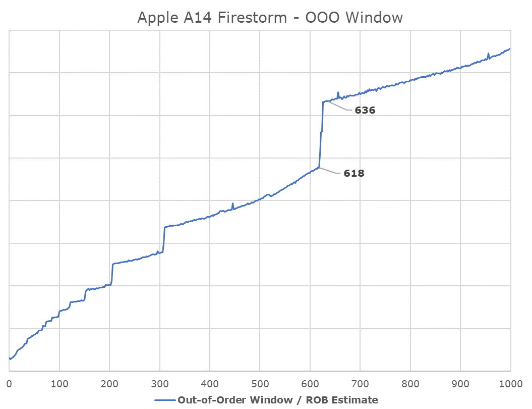
One aspect of recent Apple designs which we were never really able to answer concretely is how deep their out-of-order execution capabilities are. The last official resource we had on the matter was a 192 figure for the ROB (Re-order Buffer) inside of the 2013 Cyclone design. Thanks again to Veedrac’s implementation of a test that appears to expose this part of the µarch, we can seemingly confirm that Firestorm’s ROB is in the 630 instruction range deep, which had been an upgrade from last year’s A13 Lightning core which is measured in at 560 instructions. It’s not clear as to whether this is actually a traditional ROB as in other architectures, but the test at least exposes microarchitectural limitations which are tied to the ROB and behaves and exposes correct figures on other designs in the industry. An out-of-order window is the amount of instructions that a core can have “parked”, waiting for execution in, well, out of order sequence, whilst the core is trying to fetch and execute the dependencies of each instruction.
A +-630 deep ROB is an immensely huge out-of-order window for Apple’s new core, as it vastly outclasses any other design in the industry. Intel’s Sunny Cove and Willow Cove cores are the second-most “deep” OOO designs out there with a 352 ROB structure, while AMD’s newest Zen3 core makes due with 256 entries, and recent Arm designs such as the Cortex-X1 feature a 224 structure.
Exactly how and why Apple is able to achieve such a grossly disproportionate design compared to all other designers in the industry isn’t exactly clear, but it appears to be a key characteristic of Apple’s design philosophy and method to achieve high ILP (Instruction level-parallelism).
Many, Many Execution Units
Having high ILP also means that these instructions need to be executed in parallel by the machine, and here we also see Apple’s back-end execution engines feature extremely wide capabilities. On the Integer side, whose in-flight instructions and renaming physical register file capacity we estimate at around 354 entries, we find at least 7 execution ports for actual arithmetic operations. These include 4 simple ALUs capable of ADD instructions, 2 complex units which feature also MUL (multiply) capabilities, and what appears to be a dedicated integer division unit. The core is able to handle 2 branches per cycle, which I think is enabled by also one or two dedicated branch forwarding ports, but I wasn’t able to 100% confirm the layout of the design here.
The Firestorm core here doesn’t appear to have major changes on the Integer side of the design, as the only noteworthy change was an apparent slight increase (yes) in the integer division latency of that unit.
On the floating point and vector execution side of things, the new Firestorm cores are actually more impressive as they a 33% increase in capabilities, enabled by Apple’s addition of a fourth execution pipeline. The FP rename registers here seem to land at 384 entries, which is again comparatively massive. The four 128-bit NEON pipelines thus on paper match the current throughput capabilities of desktop cores from AMD and Intel, albeit with smaller vectors. Floating-point operations throughput here is 1:1 with the pipeline count, meaning Firestorm can do 4 FADDs and 4 FMULs per cycle with respectively 3 and 4 cycles latency. That’s quadruple the per-cycle throughput of Intel CPUs and previous AMD CPUs, and still double that of the recent Zen3, of course, still running at lower frequency. This might be one reason why Apples does so well in browser benchmarks (JavaScript numbers are floating-point doubles).
Vector abilities of the 4 pipelines seem to be identical, with the only instructions that see lower throughput being FP divisions, reciprocals and square-root operations that only have an throughput of 1, on one of the four pipes.
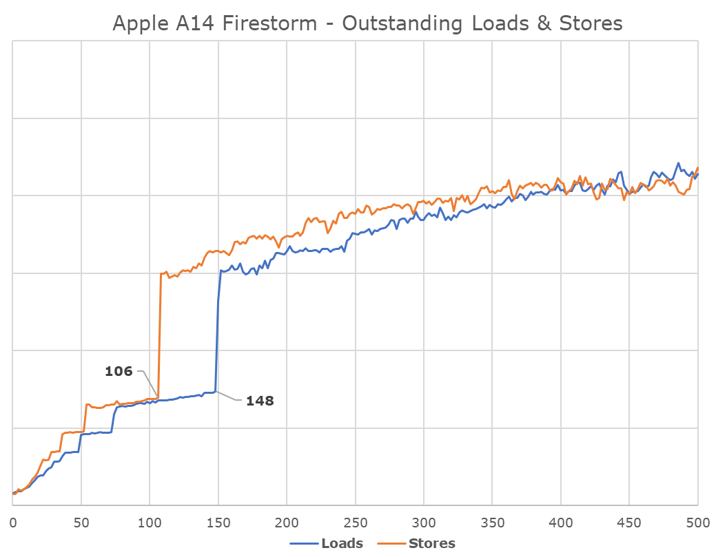
On the load-store front, we’re seeing what appears to be four execution ports: One load/store, one dedicated store and two dedicated load units. The core can do at max 3 loads per cycle and two stores per cycle, but a maximum of only 2 loads and 2 stores concurrently.
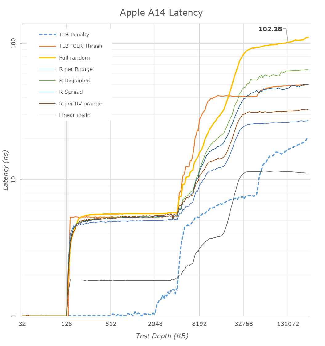
What’s interesting here is again the depth of which Apple can handle outstanding memory transactions. We’re measuring up to around 148-154 outstanding loads and around 106 outstanding stores, which should be the equivalent figures of the load-queues and store-queues of the memory subsystem. To not surprise, this is also again deeper than any other microarchitecture on the market. Interesting comparisons are AMD’s Zen3 at 44/64 loads & stores, and Intel’s Sunny Cove at 128/72. The Intel design here isn’t far off from Apple and actually the throughput of these latest microarchitecture is relatively matched – it would be interesting to see where Apple is going to go once they deploy the design to non-mobile memory subsystems and DRAM.
One large improvement on the part of the Firestorm cores this generation has been on the side of the TLBs. The L1 TLB has been doubled from 128 pages to 256 pages, and the L2 TLB goes up from 2048 pages to 3072 pages. On today’s iPhones this is an absolutely overkill change as the page size is 16KB, which means that the L2 TLB covers 48MB which is well beyond the cache capacity of even the A14. With Apple moving the microarchitecture onto Mac systems, having compatibility with 4KB pages and making sure the design still offers enough performance would be a key part as to why Apple chose to make such a large upgrade this generation.
On the cache hierarchy side of things, we’ve known for a long time that Apple’s designs are monstrous, and the A14 Firestorm cores continue this trend. Last year we had speculated that the A13 had 128KB L1 Instruction cache, similar to the 128KB L1 Data cache for which we can test for, however following Darwin kernel source dumps Apple has confirmed that it’s actually a massive 192KB instruction cache. That’s absolutely enormous and is 3x larger than the competing Arm designs, and 6x larger than current x86 designs, which yet again might explain why Apple does extremely well in very high instruction pressure workloads, such as the popular JavaScript benchmarks.
The huge caches also appear to be extremely fast – the L1D lands in at a 3-cycle load-use latency. We don’t know if this is clever load-load cascading such as described on Samsung’s cores, but in any case, it’s very impressive for such a large structure. AMD has a 32KB 4-cycle cache, whilst Intel’s latest Sunny Cove saw a regression to 5 cycles when they grew the size to 48KB. Food for thought on the advantages or disadvantages of slow of fast frequency designs.
On the L2 side of things, Apple has been employing an 8MB structure that’s shared between their two big cores. This is an extremely unusual cache hierarchy and contrasts to everybody else’s use of an intermediary sized private L2 combined with a larger slower L3. Apple here disregards the norms, and chooses a large and fast L2. Oddly enough, this generation the A14 saw the L2 of the big cores make a regression in terms of access latency, going back from 14 cycles to 16 cycles, reverting the improvements that had been made with the A13. We don’t know for sure why this happened, I do see higher parallel access bandwidth into the cache for scalar workloads, however peak bandwidth still seems to be the same as the previous generation. Another point of hypothesis is that because Apple shares the L2 amongst cores, that this might be an indicator of changes for Apple Silicon SoCs with more than just two cores connected to a single cache, much like the A12X generation.
Apple has had employed a large LLC on their SoCs for many generations now. On the A14 this appears to be again a 16MB cache that is serving all the IP blocks on the SoC, most useful of course for the CPU and GPU. Comparatively speaking, this cache hierarchy isn’t nearly as fast as the actual CPU-cluster L3s of other designs out there, and in recent years we’ve seen more mobile SoC vendors employ such LLC in front of the memory controllers for the sake of power efficiency. What Apple would do in a larger laptop or desktop chip remains unclear, but I do think we’d see similar designs there.
We’ve covered more specific aspects of Apple’s designs, such as their MLP (memory level parallelism) capabilities, and the A14 doesn’t seem to change in that regard. One other change I’ve noted from the A13 is that the new design now also makes usage of Arm’s more relaxed memory model in that the design is able to optimise streaming stores into non-temporal stores automatically, mimicking the change that had been introduced in the Cortex-A76 and the Exynos-M4. x86 designs wouldn’t be able to achieve a similar optimization in theory – at least it would be very interesting to see if one attempted to do so.
| Maximum Frequency vs Loaded Threads Per-Core Maximum MHz |
||||||
| Apple A14 | 1 | 2 | 3 | 4 | 5 | 6 |
| Performance 1 | 2998 | 2890 | 2890 | 2890 | 2890 | 2890 |
| Performance 2 | 2890 | 2890 | 2890 | 2890 | 2890 | |
| Efficiency 1 | 1823 | 1823 | 1823 | 1823 | ||
| Efficiency 2 | 1823 | 1823 | 1823 | |||
| Efficiency 3 | 1823 | 1823 | ||||
| Efficiency 4 | 1823 | |||||
Of course, the old argument about having a very wide architecture is that you cannot clock as high as something which is narrower. This is somewhat true; however, I wouldn’t come to any conclusion as to the capabilities of Apple’s design in a higher power device. On the A14 inside of the new iPhones the new Firestorm cores are able to reach 3GHz clock speeds, clocking down to 2.89GHz when there’s two cores active at any time.
We’ll be investigating power in more detail in just a bit, but I currently see Apple being limited by the thermal envelope of the actual phones rather than it being some intrinsic clock ceiling of the microarchitecture. The new Firestorm cores are clocking in now at roughly the same speed any other mobile CPU microarchitecture from Arm even though it’s a significantly wider design – so the argument about having to clock slower because of the more complex design also doesn’t seem to apply in this instance. It will be very interesting to see what Apple could do not only in a higher thermal envelope device such as a laptop, but also on a wall-powered device such as a Mac.


644 Comments
View All Comments
29a - Thursday, November 12, 2020 - link
Folks are people, bit you probably knew that.CharonPDX - Saturday, November 14, 2020 - link
My sister has needed a new laptop for a while - she has a Windows laptop now, but her work laptop is an Apple, and she likes Apple. (She's a government employee, so *CAN'T* use her work laptop for personal uses.)So, ordered a MacBook Air for her for Christmas (splitting the cost with our parents.)
While I was at it, ordered myself a Mini to play with, and probably replace my old 2012 Mini in "home server" use.
Alej - Saturday, November 14, 2020 - link
There’s a running theme on twitter and on a thread on Blender artists forums where they point out that the unique memory and texture compressions available to the M1 chip memory hardware would allow it to fit scenes with 100+GB of textures inside those 16GB for GPU rendering.Apple for a long time has touted that they have clever RAM management at the OS level and I truly believe it, I can use an 8GB 2015 MacBook for light-to-mid work and it’s pleasant while using a Windows Laptop with the same 8GB can prove sluggish even when just doing browser navigation (although many other variables for that to happen besides being actually the memory available).
mdriftmeyer - Saturday, December 5, 2020 - link
Must be some mysterious Fractal Compression [bs] to pull off that fantastical feat of creative story telling.mattbe - Saturday, November 14, 2020 - link
"not when ssd of today is *faster* than memory of even a few years ago."This is simply not correct. Please show me an example where SSD is faster than memory (DDR4) from a few years ago.
alysdexia - Wednesday, November 11, 2020 - link
faster -> swiftlier; Macbook -> MacBook; will -> shalladt6247 - Thursday, November 12, 2020 - link
But regardless of OS, some workloads need more RAM. It's why I jumped ship from Mac laptops a couple generations ago. In situations where I'm running tons of VMs and Docker images, building enterprise Java apps, etc. that 16GB of RAM get chewed through real quick.It's not to say that 16GB isn't good enough for most people -- it certainly is. But in 2020, calling it a "Pro" laptop and unable to handle certain classes of increasingly common professional workloads is not great. That being said, this is a first step. It's clear they're going to have to go to RAM off-package for some machines (at least the Mac Pro), hopefully that will trickle down to the Pro laptops.
Also, I'd LOVE to see Linux distros targeting this hardware. Should be fun to run some benchmarks.
danbob999 - Friday, November 13, 2020 - link
The required RAM has nothing to do with the architecture.ARM requires as much RAM as x86 to run the same applications. No reason why macOS would use half the RAM with Apple silicon. With universal binaries taking more space, RAM usage could even go up a bit.
NetMage - Friday, November 13, 2020 - link
Universal binaries may need more storage but there is no reason they should need more RAM.alysdexia - Wednesday, November 11, 2020 - link
a iPad Pro version?