NVIDIA Unveils Grace: A High-Performance Arm Server CPU For Use In Big AI Systems
by Ryan Smith on April 12, 2021 12:20 PM EST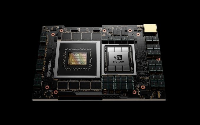
Kicking off another busy Spring GPU Technology Conference for NVIDIA, this morning the graphics and accelerator designer is announcing that they are going to once again design their own Arm-based CPU/SoC. Dubbed Grace – after Grace Hopper, the computer programming pioneer and US Navy rear admiral – the CPU is NVIDIA’s latest stab at more fully vertically integrating their hardware stack by being able to offer a high-performance CPU alongside their regular GPU wares. According to NVIDIA, the chip is being designed specifically for large-scale neural network workloads, and is expected to become available in NVIDIA products in 2023.
With two years to go until the chip is ready, NVIDIA is playing things relatively coy at this time. The company is offering only limited details for the chip – it will be based on a future iteration of Arm’s Neoverse cores, for example – as today’s announcement is a bit more focused on NVIDIA’s future workflow model than it is speeds and feeds. If nothing else, the company is making it clear early on that, at least for now, Grace is an internal product for NVIDIA, to be offered as part of their larger server offerings. The company isn’t directly gunning for the Intel Xeon or AMD EPYC server market, but instead they are building their own chip to complement their GPU offerings, creating a specialized chip that can directly connect to their GPUs and help handle enormous, trillion parameter AI models.
| NVIDIA SoC Specification Comparison | |||||
| Grace | Xavier | Parker (Tegra X2) |
|||
| CPU Cores | ? | 8 | 2 | ||
| CPU Architecture | Next-Gen Arm Neoverse (Arm v9?) |
Carmel (Custom Arm v8.2) |
Denver 2 (Custom Arm v8) |
||
| Memory Bandwidth | >500GB/sec LPDDR5X (ECC) |
137GB/sec LPDDR4X |
60GB/sec LPDDR4 |
||
| GPU-to-CPU Interface | >900GB/sec NVLink 4 |
PCIe 3 | PCIe 3 | ||
| CPU-to-CPU Interface | >600GB/sec NVLink 4 |
N/A | N/A | ||
| Manufacturing Process | ? | TSMC 12nm | TSMC 16nm | ||
| Release Year | 2023 | 2018 | 2016 | ||
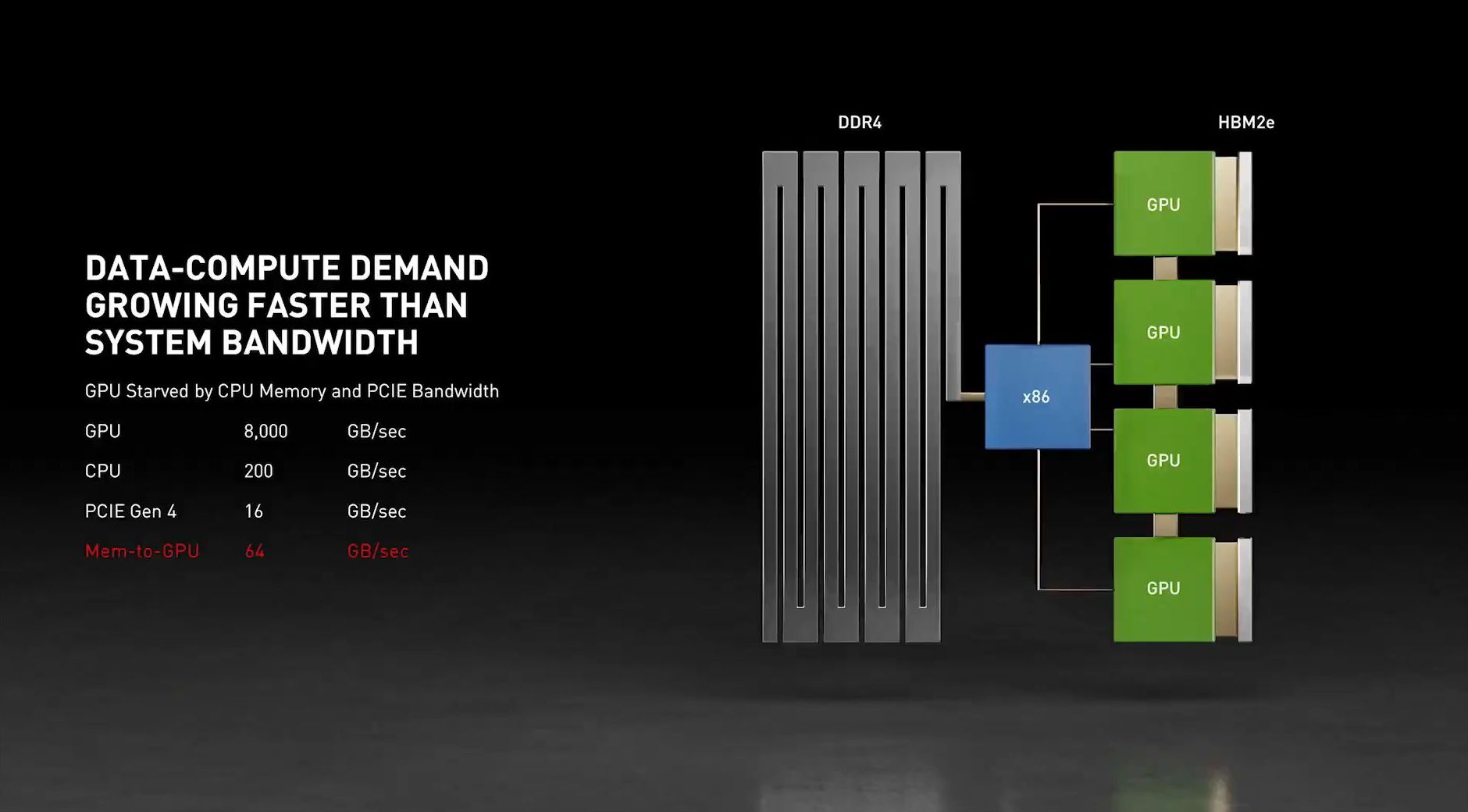
More broadly speaking, Grace is designed to fill the CPU-sized hole in NVIDIA’s AI server offerings. The company’s GPUs are incredibly well-suited for certain classes of deep learning workloads, but not all workloads are purely GPU-bound, if only because a CPU is needed to keep the GPUs fed. NVIDIA’s current server offerings, in turn, typically rely on AMD’s EPYC processors, which are very fast for general compute purposes, but lack the kind of high-speed I/O and deep learning optimizations that NVIDIA is looking for. In particular, NVIDIA is currently bottlenecked by the use of PCI Express for CPU-GPU connectivity; their GPUs can talk quickly amongst themselves via NVLink, but not back to the host CPU or system RAM.
The solution to the problem, as was the case even before Grace, is to use NVLink for CPU-GPU communications. Previously NVIDIA has worked with the OpenPOWER foundation to get NVLink into POWER9 for exactly this reason, however that relationship is seemingly on its way out, both as POWER’s popularity wanes and POWER10 is skipping NVLink. Instead, NVIDIA is going their own way by building an Arm server CPU with the necessary NVLink functionality.
The end result, according to NVIDIA, will be a high-performance and high-bandwidth CPU that is designed to work in tandem with a future generation of NVIDIA server GPUs. With NVIDIA talking about pairing each NVIDIA GPU with a Grace CPU on a single board – similar to today’s mezzanine cards – not only does CPU performance and system memory scale up with the number of GPUs, but in a roundabout way, Grace will serve as a co-processor of sorts to NVIDIA’s GPUs. This, if nothing else, is a very NVIDIA solution to the problem, not only improving their performance, but giving them a counter should the more traditionally integrated AMD or Intel try some sort of similar CPU+GPU fusion play.
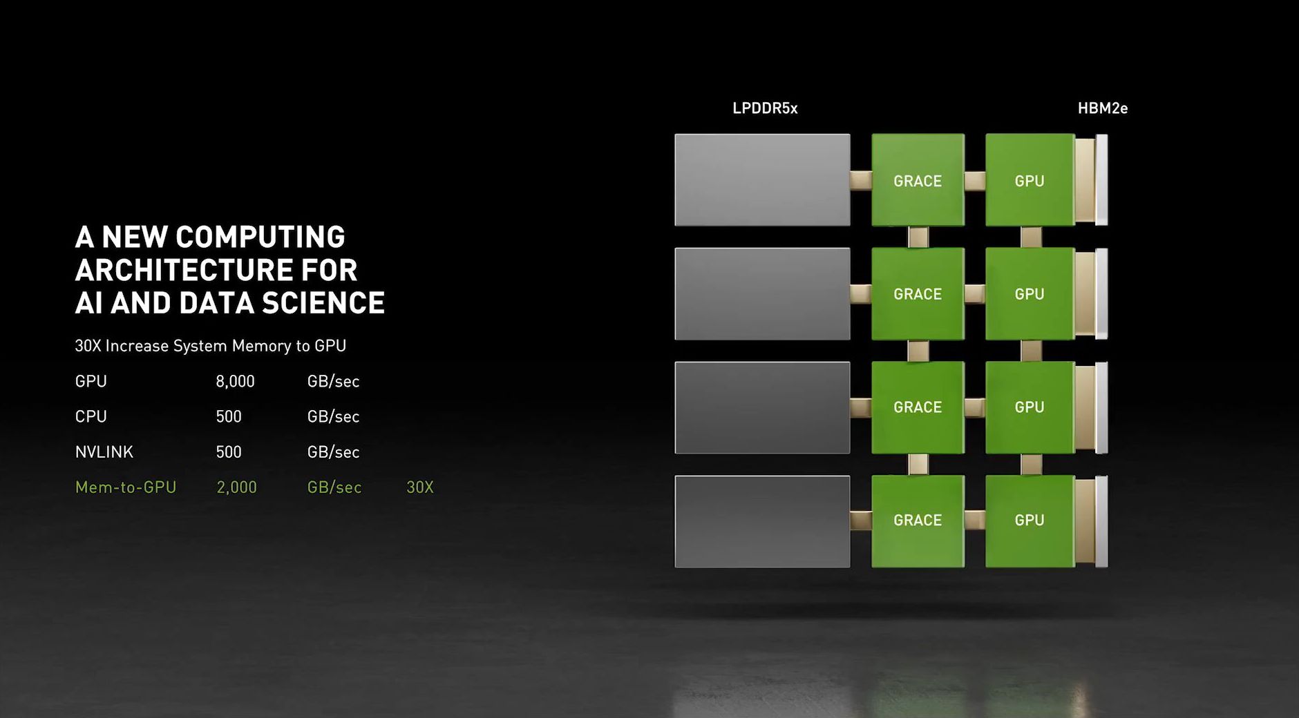
By 2023 NVIDIA will be up to NVLink 4, which will offer at least 900GB/sec of cummulative (up + down) bandwidth between the SoC and GPU, and over 600GB/sec cummulative between Grace SoCs. Critically, this is greater than the memory bandwidth of the SoC, which means that NVIDIA’s GPUs will have a cache coherent link to the CPU that can access the system memory at full bandwidth, and also allowing the entire system to have a single shared memory address space. NVIDIA describes this as balancing the amount of bandwidth available in a system, and they’re not wrong, but there’s more to it. Having an on-package CPU is a major means towards increasing the amount of memory NVIDIA’s GPUs can effectively access and use, as memory capacity continues to be the primary constraining factors for large neural networks – you can only efficiently run a network as big as your local memory pool.
| CPU & GPU Interconnect Bandwidth | |||||
| Grace | EPYC 2 + A100 | EPYC 1 + V100 | |||
| GPU-to-CPU Interface (Cummulative, Both Directions) |
>900GB/sec NVLink 4 |
~64GB/sec PCIe 4 x16 |
~32GB/sec PCIe 3 x16 |
||
| CPU-to-CPU Interface (Cummulative, Both Directions) |
>600GB/sec NVLink 4 |
304GB/sec Infinity Fabric 2 |
152GB/sec Infinity Fabric |
||
And this memory-focused strategy is reflected in the memory pool design of Grace, as well. Since NVIDIA is putting the CPU on a shared package with the GPU, they’re going to put the RAM down right next to it. Grace-equipped GPU modules will include a to-be-determined amount of LPDDR5x memory, with NVIDIA targeting at least 500GB/sec of memory bandwidth. Besides being what’s likely to be the highest-bandwidth non-graphics memory option in 2023, NVIDIA is touting the use of LPDDR5x as a gain for energy efficiency, owing to the technology’s mobile-focused roots and very short trace lengths. And, since this is a server part, Grace’s memory will be ECC-enabled, as well.
As for CPU performance, this is actually the part where NVIDIA has said the least. The company will be using a future generation of Arm’s Neoverse CPU cores, where the initial N1 design has already been turning heads. But other than that, all the company is saying is that the cores should break 300 points on the SPECrate2017_int_base throughput benchmark, which would be comparable to some of AMD’s second-generation 64 core EPYC CPUs. The company also isn’t saying much about how the CPUs are configured or what optimizations are being added specifically for neural network processing. But since Grace is meant to support NVIDIA’s GPUs, I would expect it to be stronger where GPUs in general are weaker.
Otherwise, as mentioned earlier, NVIDIA big vision goal for Grace is significantly cutting down the time required for the largest neural networking models. NVIDIA is gunning for 10x higher performance on 1 trillion parameter models, and their performance projections for a 64 module Grace+A100 system (with theoretical NVLink 4 support) would be to bring down training such a model from a month to three days. Or alternatively, being able to do real-time inference on a 500 billion parameter model on an 8 module system.
Overall, this is NVIDIA’s second real stab at the data center CPU market – and the first that is likely to succeed. NVIDIA’s Project Denver, which was originally announced just over a decade ago, never really panned out as NVIDIA expected. The family of custom Arm cores was never good enough, and never made it out of NVIDIA’s mobile SoCs. Grace, in contrast, is a much safer project for NVIDIA; they’re merely licensing Arm cores rather than building their own, and those cores will be in use by numerous other parties, as well. So NVIDIA’s risk is reduced to largely getting the I/O and memory plumbing right, as well as keeping the final design energy efficient.
If all goes according to plan, expect to see Grace in 2023. NVIDIA is already confirming that Grace modules will be available for use in HGX carrier boards, and by extension DGX and all the other systems that use those boards. So while we haven’t seen the full extent of NVIDIA’s Grace plans, it’s clear that they are planning to make it a core part of future server offerings.
First Two Supercomputer Customers: CSCS and LANL
And even though Grace isn’t shipping until 2023, NVIDIA has already lined up their first customers for the hardware – and they’re supercomputer customers, no less. Both the Swiss National Supercomputing Centre (CSCS) and Los Alamos National Laboratory are announcing today that they’ll be ordering supercomputers based on Grace. Both systems will be built by HPE’s Cray group, and are set to come online in 2023.
CSCS’s system, dubbed Alps, will be replacing their current Piz Daint system, a Xeon plus NVIDIA P100 cluster. According to the two companies, Alps will offer 20 ExaFLOPS of AI performance, which is presumably a combination of CPU, CUDA core, and tensor core throughput. When it’s launched, Alps should be the fastest AI-focused supercomputer in the world.
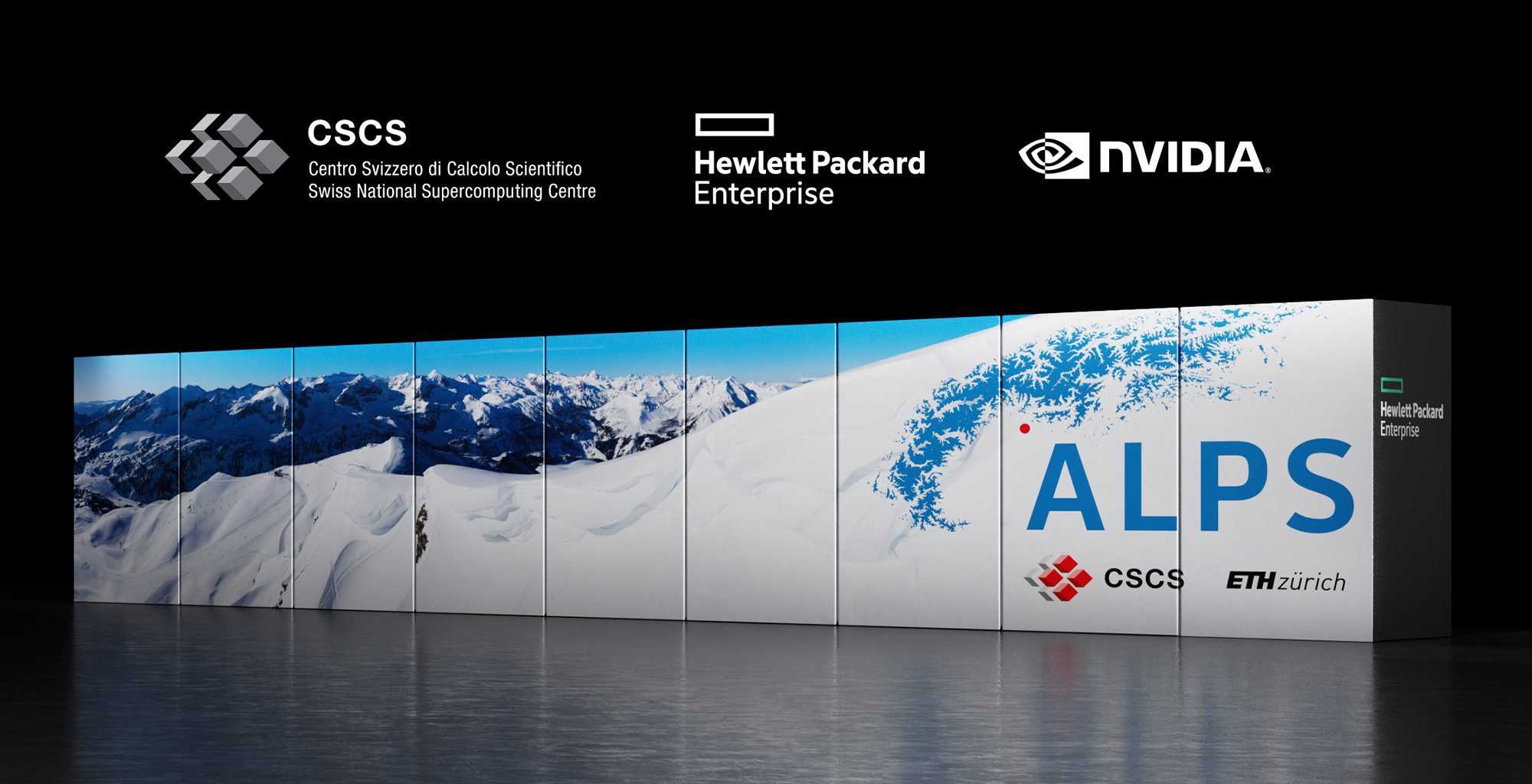
An artist's rendition of the expected Alps system
Interestingly, however, CSCS’s ambitions for the system go beyond just machine learning workloads. The institute says that they’ll be using Alps as a general purpose system, working on more traditional HPC-type tasks as well as AI-focused tasks. This includes CSCS’s traditional research into weather and the climate, which the pre-AI Piz Daint is already used for as well.
As previously mentioned, Alps will be built by HPE, who will be basing on their previously-announced Cray EX architecture. This would make NVIDIA’s Grace the second CPU option for Cray EX, along with AMD’s EPYC processors.
Meanwhile Los Alamos’ system is being developed as part of an ongoing collaboration between the lab and NVIDIA, with LANL set to be the first US-based customer to receive a Grace system. LANL is not discussing the expected performance of their system beyond the fact that it’s expected to be “leadership-class,” though the lab is planning on using it for 3D simulations, taking advantage of the largest data set sizes afforded by Grace. The LANL system is set to be delivered in early 2023.


119 Comments
View All Comments
SarahKerrigan - Monday, April 12, 2021 - link
Once upon a time, there was a lot of talk about Denver cores being integrated into at least some Maxwell family products. I don't know if it was ever an actual program in Nvidia, and if so, what ended up happening (though Denver performance was not amazing, and that may have played into it.)mode_13h - Wednesday, April 14, 2021 - link
Tegra X2 has Denver cores and Pascal GPU. That's probably what you heard about. It launched in like 2016.SarahKerrigan - Wednesday, April 14, 2021 - link
It's not. :) I was at the X2's Hot Chips presentation; I remember it in considerable detail, and would not mix that up.For a while, the rumor mill pointed heavily to Denver cores being integrated into either first-gen or second-gen Maxwell dGPUs to avoid the roundtrip back to the host for compute loads. Looking back about the articles about it, it looks like it was a combination of false rumors and probable misinterpretation of an Nvidia exec's comment that "the Maxwell generation will be the first end-product using Project Denver" (which was not the case, but was indicated by roadmaps for a bit.)
mode_13h - Thursday, April 15, 2021 - link
Some of the Tegra chips shipped in multiple flavors that varied in terms of whether they used ARM-designed cores or Nvidia's custom cores, such as the K1However, according to this, the X2 featured 2x Denver + 4x A57 cores: https://en.wikipedia.org/wiki/Tegra#Tegra_X2
If you need further proof, here's a discussion of 3rd party developers actually comparing the performance of the Denver cores to the A57s: https://forums.developer.nvidia.com/t/denver-2-vs-...
Anyway, Tegra X1 was Maxwell-based. So, maybe the plan was to ship it with Denver cores, but they weren't done in time. One way or another, I really think those comments must've been referring to Tegra.
michael2k - Tuesday, April 13, 2021 - link
Tegra was their integrated CPU/GPU part. I imagine if they wanted to flip the script and embed 8 CPU and 1024 CUDA cores per Big.Little they could.CiccioB - Tuesday, April 13, 2021 - link
I was thinking for those CPU cores as specialized "serial cores" for the GPU. Something like a core for each GPC, a are PolyMorph Engines.Each of those cores could be a "master" manager for some work (like resource handling, thread manager, wave organizer in spite of fixed HW schedulers) or be a slave core like an RT core, for example. Or have two for both tasks.
That could improve GPU execution of serial code (which they are weak to) and better management "on die" instead of CPU drivers (that are on the other side of the PCI bus with limited bandwidth and high latency).
mode_13h - Wednesday, April 14, 2021 - link
Grace is their solution. Upgrade the CPU-GPU interconnect not only for better cooperation, but also giving the GPU better access to CPU memory.Plus, it's not like there's die space to spare, on a GPU.
eva02langley - Monday, April 12, 2021 - link
This was one hour and half of pure garbage. Nvidia saying they will do things, and in the end they are just selling GPUs.-AV are a long way to go and VIDEO is NOT the answer
-BMW video game was nothing more than a pet project joke
-Nvidia is creating a CPU... but use AWS Gravitron CPU... which are nothing beside Sagemaster run on for AI...
-Maxine.... euuhhhhhh.... no coments....
1 hour and half of dirt at the wall expecting something stick... and the dumb stakeholders bite on it. It is disgusting.
anonomouse - Monday, April 12, 2021 - link
...who hurt you?CiccioB - Tuesday, April 13, 2021 - link
simply... envy