TSMC Readies Five 3nm Process Technologies, Adds FinFlex For Design Flexibility
by Anton Shilov on June 16, 2022 3:10 PM EST
Taiwan Semiconductor Manufacturing Co. on Thursday kicked off its 2022 TSMC Technology Symposium, where the company traditionally shares it process technology roadmaps as well as its future expansion plans. One of the key things that TSMC is announcing today are its leading-edge nodes that belong to its N3 (3 nm class) and N2 (2nm class) families that will be used to make advanced CPUs, GPUs, and SoCs in the coming years.
N3: Five Nodes Over Next Three Years
As fabrication processes get more complex, their pathfinding, research, and development times get stretched out as well, so we no longer see a brand-new node emerging every two years from TSMC and other foundries. With N3, TSMC's new node introduction cadence is going to expand to around 2.5 years, whereas with N2, it will stretch to around three years.
This means that TSMC will need to offer enhanced versions of N3 in order to meet the needs of its customers who are still looking for a performance per watt improvement as well as transistor density bump every year or so. Another reason why TSMC and its customers need multiple versions of N3 is because the foundry's N2 relies on all-new gate-all-around field-effect transistors (GAA FETs) implemented using nanosheets, which is expected to come with higher costs, new design methodologies, new IP, and many other changes. While developers of bleeding-edge chips will be quick to jump to N2, many of TSMC's more rank & file customers will stick to various N3 technologies for years to come.
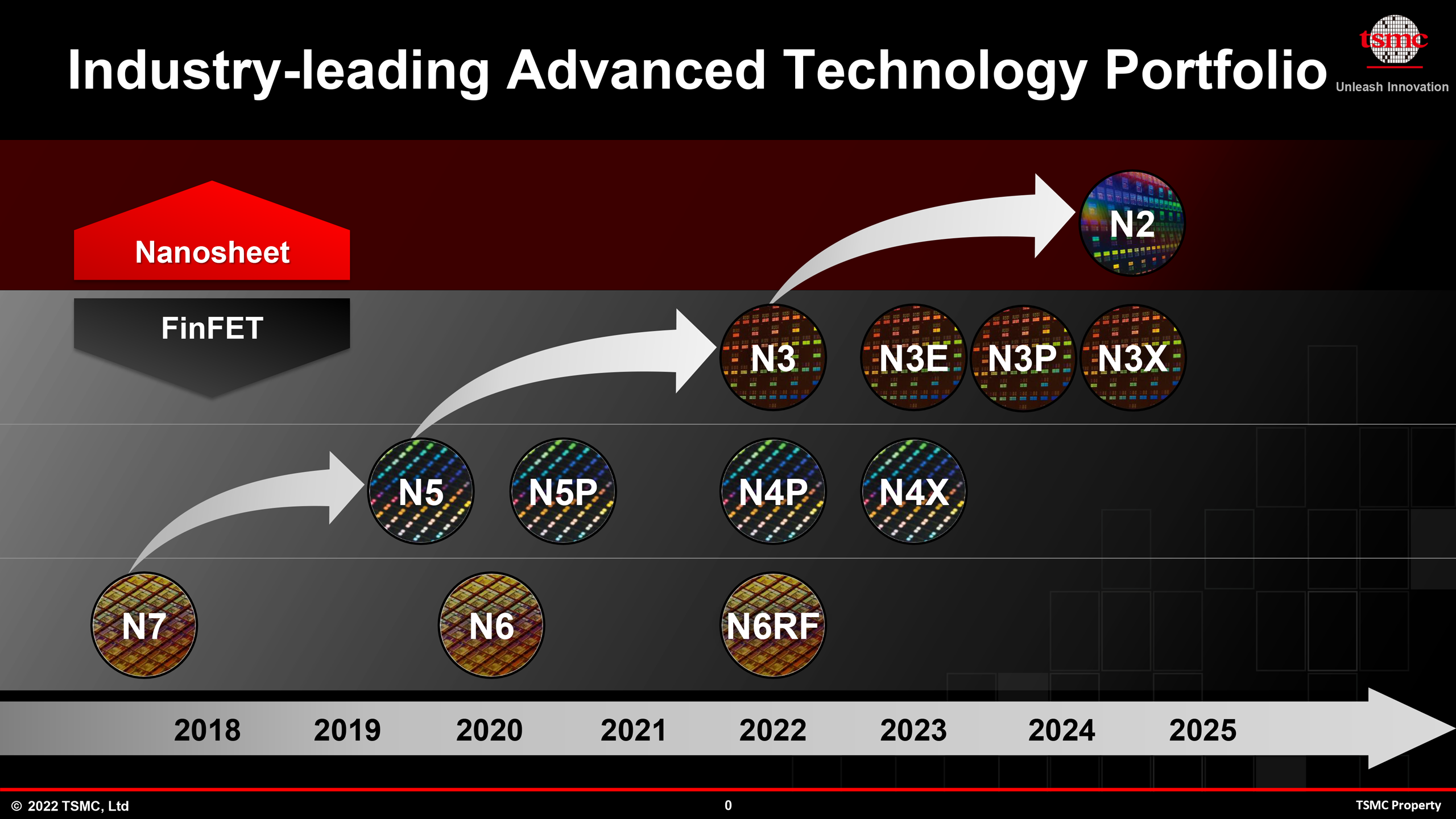
At its TSMC Technology Symposium 2022, the foundry talked about four N3-derived fabrication processes (for a total of five 3 nm-class nodes) — N3E, N3P, N3S, and N3X — set to be introduced over the coming years. These N3 variants are slated to deliver improved process windows, higher performance, increased transistor densities, and augmented voltages for ultra-high-performance applications. All these technologies will support FinFlex, a TSMC "secret sauce" feature that greatly enhances their design flexibility and allows chip designers to precisely optimize performance, power consumption, and costs.
| Advertised PPA Improvements of New Process Technologies Data announced during conference calls, events, press briefings and press releases |
||||||||
| TSMC | ||||||||
| N4 vs N5 |
N4P vs N5 |
N4P vs N4 |
N4X vs N5 |
N4X vs N4P |
N3 vs N5 |
N3E vs N5 |
||
| Power | lower | -22% | - | ? | ? | -25-30% | -34% | |
| Performance | higher | +11% | +6% | +15% or more |
+4% or more |
+10-15% | +18% | |
| Logic Area Reduction* % Logic Density* |
0.94x -6% 1.06x |
0.94x -6% 1.06x |
- |
? |
? |
0.58x -42% 1.7x |
0.625x -37.5% 1.6x |
|
| Volume Manufacturing |
2022 | 2023 | H2 2022 | 2023 | 2023 | H2 2022 | Q2/Q3 2023 | |
*Note that TSMC only started to publish transistor density enhancements for analog, logic, and SRAM separately around 2020. Some of the numbers still reflect 'mixed' density consisting of 50% logic, 30% SRAM, and 20% analog.
N3 and N3E: On Track for HVM
TSMC's first 3 nm-class node is called N3 and this one is on track to start high volume manufacturing (HVM) in the second half of this year. Actual chips are set to be delivered to customers in early 2023.This technology is mostly aimed at early adopters (read: Apple and the like) who can invest in leading-edge designs and would benefit from the performance, power, area (PPA) advantages offered by leading-edge nodes. But as it's tailored for particular types of applications, N3 has a relatively narrow process window (a range of parameters that produce a defined result), which may not be suitable for all applications in terms of yields.
This is when N3E comes into play. The new technology enhances performance, lowers power, and increases the process window, which results in higher yields. But the trade-off is that the node features a slightly reduced logic density. When compared to N5, N3E will offer a 34% reduction in power consumption (at the same speed and complexity) or an 18% performance improvement (at the same power and complexity), and will increase logic transistor density by 1.6x.
It is noteworthy that, based on data from TSMC, N3E will offer higher clockspeeds than even N4X (due in 2023). However the latter will also support ultra-high drive currents and voltages of above 1.2V, at which point it will be able to offer unbeatable performance, but with very high power consumption.
In general, N3E looks to be a more versatile node than N3, which is why it is not surprising that TSMC has more '3nm tape outs' at this point than it had with its 5 nm-class node at a similar point of its development.
Risk production of chips using N3E is set to start in the coming weeks (i.e., in Q2 or Q3 2022) with HVM set for mid-2023 (again, TSMC does not disclose whether we are talking about Q2 or Q3). So expect commercial N3E chips to be available in late 2023 or early 2024.
N3P, N3S, and N3X: Performance, Density, Voltages
N3's improvements do not stop with N3E. TSMC is set to bring out N3P, a performance-enhanced version of its fabrication process, as well as N3S, density-enhancing flavor of this node, some time around 2024. Unfortunately, TSMC is not currently disclosing what improvements these variants will offer compared to baseline N3. In fact, at its Technology Symposium 2022, TSMC did not even show N3S in its roadmap and it only got mentioned by Kevin Zhang in a conversation. Bearing all this in mind, it is really not a good business to try guessing characteristics of N3S.
Finally, for those customers who need ultra-high performance no matter power consumption and costs, TSMC will offer N3X, which is essentially an ideological successor of N4X. Again, TSMC is not revealing details about this node other than that it will support high drive currents and voltages. We might speculate that N4X could use backside power delivery, but since we are talking about a FinFET-based node and TSMC only going to implement backside power rail in nanosheet-based N2, we are not sure this is the case. Nonetheless, TSMC probably has a number of aces up its sleeve when it comes to voltage increases and performance enhancements.
FinFlex: N3's Secret Sauce
Speaking of enhancements, we should definitely mention TSMC's secret sauce for N3: FinFlex technology. In short, FinFlex allows chip designers to precisely tailor their building blocks for higher performance, higher density, and lower power.
Update 6/17: The initial version of the story incorrectly referred standard cells and blocks as transistors, which has been corrected.
When using a FinFET-based node, chip designers can choose between different libraries using different standard cells. A standard cell is the most basic building block that performs a Boolean logic or storage function and consists of a group of transistors and interconnects. From math point of view, the same function can be performed (with the same result) using a standard cell of different configurations. But from manufacturability and operation point of view, different standard cell configurations are characterized by different performance, power consumption, and area. When developers need to minimize die size and save power at the cost of performance, they use small standard cells. But when they need to maximize performance at the trade-off of die size and higher power, they use large standard cells.
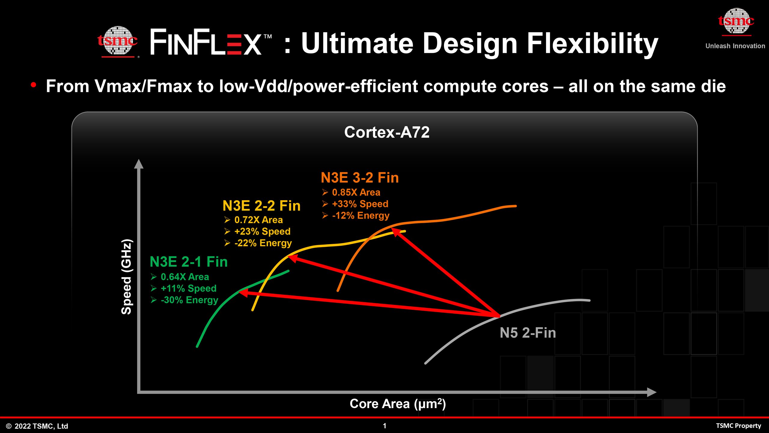
Currently, chip designers have to stick to one library/standard cells either for the whole chip or the whole block in a SoC design. For example, CPU cores can be implemented using 3-2 fin blocks to make them run faster, or 2-1 fin standard cells to reduce their power consumption and footprint. This is a fair tradeoff, but it's not ideal for all cases, especially when we are talking about 3 nm-class nodes that will be more expensive to use than existing technologies.
For N3, TSMC's FinFlex technology will allow chip designers to mix and match different kinds of standard cells within one block to precisely tailor performance, power consumption, and area. For complex structures like CPU cores, such optimizations give a lot of opportunities to increase core performance while still optimizing die sizes. So, we are eager to see how SoC designers will be able to take advantage of FinFlex in the looming N3 era.
FinFlex is not a substitute for node specialization (performance, density, voltages) as process technologies have greater differences than the ibraries or transistor structures within a single process technology, but FinFlex looks to be a good way to optimize performance, power, and costs for TSMC's N3 node. Ultimately, this technology will bring the flexibility of FinFET-based nodes a little closer to that of nanosheet/GAAFET-based nodes, which are slated to offer adjustable channel widths to get higher performance or reduce power consumption.
Summary
Like TSMC's N7 and N5, N3 will be another family of long-lasting nodes for the world's largest contrast maker of semiconductors. Especially with the jump to nanosheet-based GAAFETs coming up at 2nm for TSMC, the 3nm family will be the final family of "classic" leading-edge FinFET nodes from the firm, and one that a lot of customers will stick to for several years (or more). Which, in turn, is why TSMC is prepping multiple versions of N3 tailored for different applications – as well as FinFlex technology to give chip designers some additional flexibility with their designs.
The first N3 chips are set to enter production in the coming months and arrive to the market in early 2023. Meanwhile, TSMC will keep producing semiconductors using its N3 nodes long after it introduces its N2 process technology in 2025.


43 Comments
View All Comments
SiliconFly - Sunday, June 26, 2022 - link
Intel is using Intel 7 this year with new the HP library (v2). Might take raptor lake upto 6 GHz (with a slight increase in power draw). But will beat AMD by a mile in performance but not efficiency though.Intel is going to use Intel 4 next year which is far superior to TSMC N5 & N4 that AMD uses. In fact, the Intel 4 HP library is actually slightly better than than even the upcoming TSMC N3.
Intel is going to use Intel 20A in 2024 for it's Arrow Lake and AMD will still be using the old TSMC N3 which is one *full* node behind. AMD is going to lag both in performance AND power efficiency. Intel now leads AMD in all aspects.
Intel is going to use Intel 18A in 2025 for next gen client cpus while AMD will still be stuck in the old TSMC N3 which will now be *TWO FULL NODES* behind. Henceforth, AMD will be history.
Intel's execution woes will be over once they launch Intel 4. And its going into risk production this Q4 and volume ramp in Q2 2023.
As a contingency measure, they've also secured major N3 capacity starting 2023 & their client dies are now fully node agnostic starting 2023. They can jump to N3 anytime they wish if 20A falls behind. There no stopping Intel anymore.
dotjaz - Friday, June 17, 2022 - link
How is N3 delayed? It has always been 22H2 and unable to meet Apple's iPhone release cycle. We've known this since before 2020.dotjaz - Friday, June 17, 2022 - link
https://www.anandtech.com/show/16024/tsmc-details-...That's from nearly 2 years ago. And I'm sure earlier reports have mentioned the same timeline.
TSMC's FinFET processes have always entered HVM during Q2 and start producing Apple chips no later than early June. The earliest for N3 to actually enter mass production is August 2022 for 22H2 schedule. Why do you think Apple could possibly choose N3 and keep September/October shipping date? It's obviously not planned. Not delayed.
Blastdoor - Saturday, June 18, 2022 - link
If Intel keeps their current pace of updating their roadmaps and releasing marketing materials then poor TSMC will have no choice but to expand production and gain market share.The only real threat to TSMC is that their giant honey pot might attract the attention of a malevolent Pooh bear.
FreckledTrout - Thursday, June 23, 2022 - link
Looking at the timing N3 looks to be on time or close enough within a margin of error. Maybe not what Apple wants but on time from a TSMC perspective. What does look delayed is N2.OneEng - Monday, July 4, 2022 - link
Intel's roadmap is indeed impressive; however, 2 things give me pause.First, as techjunkie123 points out, Intel hasn't exactly been a shining beacon of execution in process technology lately (14nm +++++ anyone?).
Second, if you look carefully at both TSMC and Intel's roadmaps, they are both essentially talking about a couple really big things in the next 5 years. Gate All Around (a better implementation of multiple fins in finfets ... which I guess now we will call GalaFets? Intel likes to call it ribbon FET), and EUV (which TSMC is already doing with its N7+ and N5 nodes).
Both companies are using ASML equipment for EUV. I wouldn't bet the farm on intel out-executing TSMC in the near future IMO.
shabby - Thursday, June 16, 2022 - link
Is tsmc also expanding its fab location portfolio... as in adding fabs outside of taiwan incase west taiwan gets all pissy?Leeea - Thursday, June 16, 2022 - link
Yes, but not enough to matter.TSMCs international fabs will be enough to keep militaries going in a fight against west Taiwan, but it will not be anywhere close to meeting civilian needs.
We all will be stuck defending Taiwan from its grumpy neighbor for at least a decade to come.
nandnandnand - Thursday, June 16, 2022 - link
Samsung, Intel, GlobalFoundries, and others have fabs. I don't think TSMC is planning to stop building new fabs in Taiwan, but they are at least putting some more overseas.The U.S. seems to be ready to throw money at the problem, and we could see something interesting come out of the SkyWater-DARPA partnership.
At some point, scaling will stop and it will all be moot. Advanced fabs will catch up with each other and others will stay in their lane on older nodes more suitable for some applications.
Leeea - Friday, June 17, 2022 - link
yea, but throwing money at the problem does not catch us up to TSMC. The real value in TSMC is the people, and it will take a sustained effort for many years to develop the talent to compete.I do not think anyone expects anyone else to catch up to TSMC for at least a decade. It it not just the high end nodes either, TSMC cranks out a massive number of chips across all of its nodes.
TSMC is in everything from cars to microwaves. It is not just a matter of catching up with their high end nodes, it is matter of catching up to their massive volume.