Intel's 50Gbps Silicon Photonics Link: The Future of Interfaces
by Brian Klug on July 30, 2010 6:49 AM EST- Posted in
- Trade Shows
- Intel
- Photonics
- Laser
On Tuesday, Intel demonstrated the world’s first practical data connection using silicon photonics - a 50 gigabit per second optical data connection built around an electrically pumped hybrid silicon laser. They achieved the 50 gigabit/s data rate by multiplexing 4 12.5 gigabit/s wavelengths into one fiber - wavelength division multiplexing. Intel dubbed its demo the “50G Silicon Photonics Link.”
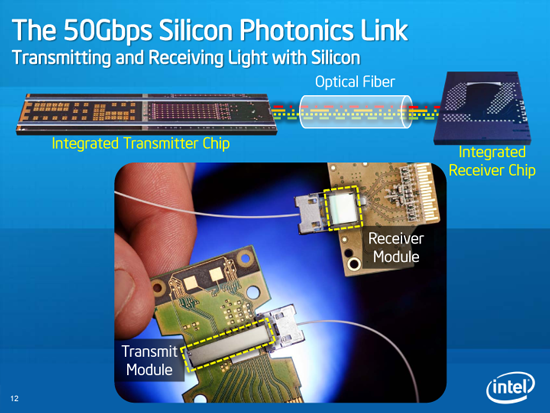
Fiber optic data transmission isn’t anything new - it’s the core of what makes the internet as we know it today possible. What makes Intel’s demonstration unique is that they’ve fabricated the laser primarily out of a low-cost, mass-produceable, highly understood material - silicon.
For years, chip designers and optical scientists alike have dreamt about the possibilities of merging traditional microelectronics and photonics. Superficially, one would expect it to be easy - after all, both fundamentally deal with electromagnetic waves, just at different frequencies (MHz and GHz for microelectronics, THz for optics).
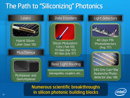
On one side, microelectronics deals with integrated circuits and components such as transistors, copper wires, and the massively understood and employed CMOS manufacturing process. It’s the backbone of microprocessors, and at the core of conventional computing today. Conversely, photonics employs - true to its name - photons, the basic unit of light. Silicon photonics is the use of optical systems that use silicon as the primary optical medium, instead of other more expensive optical materials. Eventually, photonics has the potential to supplant microelectronics with optical analogues of traditional electrical components - but that’s decades away.
Until recently, successfully integrating the two was a complex balance of manufacturing and leveraging photonics only when it was feasible. Material constraints have made photonics effective primarily as a long haul means of getting data from point to point. To a larger extent, this has made sense because copper traces on motherboards have been fast enough, but we’re getting closer and closer to the limit.


42 Comments
View All Comments
DanNeely - Friday, July 30, 2010 - link
I guess, it'd be nice to have this comment maybe include a citation to what other companies are already doing or planning on doing.Huron80 - Friday, July 30, 2010 - link
Look at Infinera, aren't they a networking provider?As stated in the article, Intel is taking what is being done effectively in Fiber Optic network transmissions - the same ones that help connect the internet - and are making a miniature version that will work inside your computer - the connections on the motherboard to components.
has407 - Friday, July 30, 2010 - link
Infinera's achievements are nothing to sneeze at, but they're quite different. AFAIK Infinera still uses a separate process for the optical components (the PIC, or "photonics IC"); they don't put everything on a single die. That's fine for certain markets, and they seem to have done well with Telecoms. However, for large scale low cost production; you're very unlikely to see it replace inter-chip or intra-chip interconnects in volume markets.Luxera is probably closer to what Intel is showing. They partnered with Freescale to integrate the photonics and electronics fab in CMOS last year to allow "low cost high volume" production"; exactly what may come from that is TBD. While we haven't seen much, Luxera's Blazar "Optical Active Cable" is a clue. But again, that's targeted at external inter-system connections; hard to tell if that's due to technology imitations or if Luxera is simply trying to generate revenue and build a market based on the technology is unclear.
In short, it's all about being able to produce everything--optical and electronic components--using a common and low cost fab. In that, Luxera/Freescale and Intel seem to be in the lead, and I'd wager Intel is most likely to bring it mainstream sooner rather than later.
This has the potential to significantly reduce the "interconnect tax" imposed by copper, which increases as speeds increase, and will soon be untenable. Intel said 20GHz was the ceiling for serial interconnects some years ago. (Teething problems related to power consumption with 10Gbe copper provide clues.) Even Inte's prediction is off by a factor of two, the end of that road is in sight.
At a guess, we'll see photonics integration in high-margin parts with the first replacing QPI as the backbone interconnect in high-end systems. Or maybe blade systems with optical backplanes. Or...
Jaybus - Friday, July 30, 2010 - link
Another thing to consider is that one reason for motherboards being as large as they are is that there must be hundreds of traces interconnecting components. Components have to be spread out to leave room for the traces. This technology will allow for one optical link to replace all of the myriad traces connecting the CPU to the northbridge, for example. Components can be closer together.Another factor is bus cards. Cards can be placed anywhere and connected by a single small fiber optic cable. Disk drives, etc. can be connected optically. This will substantially reduce the size of a full featured motherboard.
arnavvdesai - Friday, July 30, 2010 - link
While I agree components can be closer. We also have to think about the issue of heat dissipation. If we start moving items closer then we might have to deal with other issues.Jaybus - Monday, August 2, 2010 - link
Certainly, cooling will force a minimum size, but there is no reason an ATX board could not be shrunk to ITX size, at least, yet have even more i/o capability than a current ATX board. The board components could be placed as closely as is feasible, given the heat dissipation required.clarkn0va - Tuesday, August 3, 2010 - link
Doesn't replacing electrons with photons reduce the amount of heat produced?GullLars - Wednesday, August 4, 2010 - link
Not necessarily, you still need energy converting the digital electronic signal to optical and back, it's just the transport that saves energy, and only as much as the resistance in the copper wire. For high frequency or long distance information transport, it can be noticeable power savings.Regarding cooling, one quick solution is to switch the default from air cooling to liquid cooling in higher power systems. By placing the radiator, pump, and reservoir outside the system, and exploiting the new available dimension inside the case, you can make much smaller (and quieter while better cooled) systems.
Ninhalem - Friday, July 30, 2010 - link
The problem with a shrinking motherboard is that would leave too little room to put in cooling for the CPU and the memory. We're still a ways away from having CPUs running on light like the article said. I'm interested in not only shrinking the board a bit but having a different shape and orientation for the memory, video, audio card, and any other component you have in the case.Maybe have an upside down L shaped board where you can place the SATA II ports close to the hard drives and the optical drive. Maybe a start shaped board. Now that distance doesn't matter, the possibilities are endless. Very fascinating and exciting stuff.
darckhart - Friday, July 30, 2010 - link
sure, but they haven't talked about heat constraints yet.