Micron's ClearNAND: 25nm + ECC, Combats Increasing Error Rates
by Anand Lal Shimpi on December 2, 2010 12:01 AM ESTEleven months ago Intel and Micron, jointly as IMFT, announced intentions to move to 25nm NAND by the end of 2010. For the past few months, IMFT has been shipping 25nm NAND although none of it has ended up in the high performance SSDs we love to cover just yet.
The problem, as with a jump to any new manufacturing node, has to do with yields. In the microprocessor space, new processes generally mean you can’t reach your clock targets and you may use more power than you’d like. The more experience you have in working with the process the more you can get these two variables under control and eventually you have a technology you can ship to the market.
The same is true with NAND, although the vectors of improvement are a bit different. Rather than clock speed and power (although both are affected) the main focus these past few months has been increasing endurance and reducing uncorrectable bit error rate.
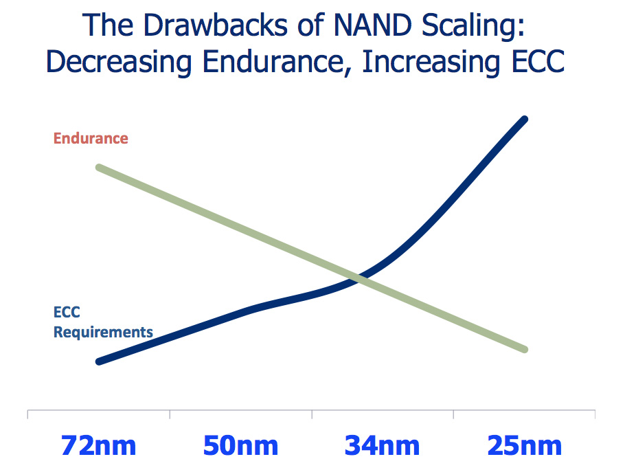
When I first started reviewing SSDs IMFT was shipping 50nm MLC NAND rated at 10,000 program/erase cycles per cell. As I mentioned in a recent SSD article, the move to 3xnm cut that endurance rating in half. Current NAND shipping in SSDs can only last half as long, or approximately 5,000 program/erase cycles per cell. Things aren’t looking any better for 25nm. Although the first 25nm MLC test parts could only manage 1,000 P/E cycles, today 25nm MLC NAND is good for around 3,000 program/erase cycles per cell.
The reduction in P/E cycles is directly related to the physics of shrinking these NAND cells; the smaller they get, the faster they deteriorate with each write. Remember this diagram?
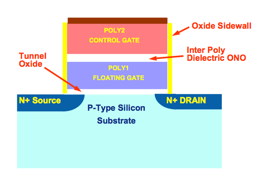
That’s an N-channel MOSFET, the building block of a NAND memory cell. Electrons travel through the tunnel oxide and make their way to the floating gate when a NAND cell is written to. The electrons are removed when a cell is erased. Each round trip is a single program/erase cycle. The process actually weakens the tunnel oxide. The smaller the tunnel oxide, the weaker it becomes, hence the decreasing p/e cycles I mentioned above.
Thankfully this doesn’t have to mean that a 3xnm SSD will die quicker than a 50nm SSD. Moore’s Law guarantees that our SSD controllers can grow in complexity and performance alongside each NAND generation. In theory, a better controller could drive write amplification lower and thus use those program/erase cycles more efficiently. This is exactly what we have seen thus far. SandForce’s SF-1200 is the perfect example of a controller-based solution to the problem of decreasing endurance with smaller geometry NAND. Even new controllers from Indilinx, Toshiba and Samsung have managed to reduce write amplification and increase performance to combat decreasing endurance.
How SandForce deals with the problem of reduced endurance and increased error rates
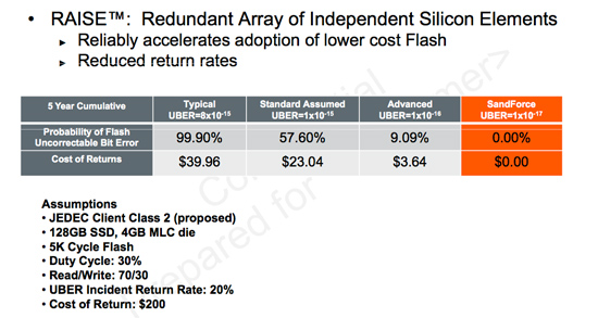
Error rates also skyrocket as a function of process geometry. The supply-demand-like curve above shows just that. SandForce integrates ECC/CRC into its controller as well as enables data redundancy across all NAND in its drives in order to combat increasing error rates with smaller geometry flash. The end result is a very forward looking, sophisticated and expensive SSD controller. What Micron plans to offer however is an alternative. It’s called ClearNAND:
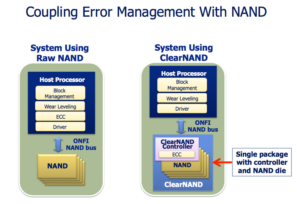
The idea is simple. Instead of placing the burden of dealing with increasing error rates on the controller, Micron will internalize the problem and equip each NAND device with an ECC controller.
The NAND will still appear to be an ONFI complaint device with the same number of pins as a regular 25nm ONFI NAND device (a single unused pin, VDDI, is now put to use in ClearNAND). The bus interface remains the same and NAND controller manufacturers don’t have to do anything differently.
On each ClearNAND device you get a 24-bit BCH ECC engine, although Micron says that in another generation or two we’ll start seeing more exotic ECC algorithms.
![]()
ClearNAND will be available starting at the 25nm node in two versions: standard and enhanced. Standard ClearNAND devices are low performance, you only get up to 50MB/s per device and up to 4 simultaneous read/write ops to the device at the same time. Enhanced ClearNAND doubles maximum capacity from 32GB to 64GB per device, quadruples interface bandwidth (200MB/s) and supports up to 16 simultaneous read/write ops. Enhanced ClearNAND would be the NAND of choice for an SSD, while Standard ClearNAND would be better suited for an iPod or smartphone for example.
Raw 25nm NAND will still be available, Micron is simply offering ClearNAND as a solution to those customers who don’t want to integrate ECC engines into their controllers.
Today the need for something like ClearNAND isn’t huge, however in the next few years Micron expects ECC equipped NAND to be the most prevalent form of NAND in the market. This would make sense as error rate goes up as process size decreases, however it does assume that the ECC requirements can’t or aren’t handled at the controller level in the future.
There’s obviously a price premium associated with ClearNAND. However since we aren’t a customer of Micron, we aren’t exactly privy to specific pricing information.
Eventually we will hit a physical wall with NAND scaling. Micron reaffirmed its commitment to research into technologies that would extend the lifespan of NAND (e.g. 3D die) or potentially augment its role in a system (e.g. phase-change memory). That’s still a few generations out though.

I don’t expect to see the first consumer SSDs to use 25nm NAND (ClearNAND or raw) until 2011. Intel’s 3rd generation X25-M will be one of the first (if not the first) and is currently scheduled to ship in Q1 2011.


24 Comments
View All Comments
NandFlashGuy - Thursday, December 2, 2010 - link
One can certainly purchase raw Nand and use a Flash programmer/reader to cycle a small portion of the Nand device and measure Raw Bit Error Rates as a function of cycle.Obviously those in the industry do this all the time.
Here's a link to a often-cited paper comparing Raw Bit Error Rates:
http://ieeexplore.ieee.org/xpls/abs_all.jsp?arnumb...
ProDigit - Sunday, December 5, 2010 - link
Interesting,if higher yields are causing more errors, I might wanna buy Intel 32nm processors NOW before the 25 nm come out with higher error rates, and lower clock speeds!
About the drives, 32nm is already pretty awesome I'd say!
I still own a 72nm ssd somewhere!
compvter - Tuesday, December 14, 2010 - link
Didn't your (or intel's) slide state that 3rd gen ssd would increase life span from 7.5TB - 15TB to 30TB - 60TB. Both have 80gb model as smallest so smallest ssd drives lifespan should go way up (4x).http://www.anandtech.com/show/3965/intels-3rd-gene...
So i wouldn't be that worried if i was planning on buying 25nm ssd.
Kevlion - Friday, December 17, 2010 - link
" today 25nm MLC NAND is good for around 3,000 program/erase cycles per cell.:"I see a lot of statistics on SSD regarding life of an SSD, and I consider myself in the extremely large mass of people still watching the SSD market to find when the value mark hits and I will take the plunge into SSD.
For the vast majority of us, SSD still don't make sense based on $ and increased performance. (Note I fully expect the ANAND readership to disagree on their personal experiences with SSD and how great they are at improving performance of their machine). However plunking down another 25% in a system build and getting 1/4 the size of a standard drive and still having to buy a standard drive as a second in the system just seems like too much at the pace the industry is changing. I mean with my last computer lasting 5 - 7 years (I know there will be those of you who groan at this) I still consider this an average life cycle for most people. That said If I plunk down this now, I need to know that it will last my 5 - 7 years. I don't want to have to re-invest in another SSD in 3 years because of decreased read/write cycles on each new generation.
All this leads to my question: What do these numbers mean to an average person like me that plays games for an hour or two every night, and uses the web for email and news???
To make an informed decision on SSD it's imparitive that we can weigh our own use versus product specs, but these numbers just are too big to make sense of... maybe there is a rule of thumb to use?