Intel Announces first 22nm 3D Tri-Gate Transistors, Shipping in 2H 2011
by Anand Lal Shimpi on May 4, 2011 2:05 PM ESTEarlier this week Intel sent us a cryptic message:
I wanted to invite you to an Intel press conference on Wednesday May 4th at 9:30am Pacific time. Intel will be making its most significant technology announcement of the year. No further details will be provided in advance. The event will be held in San Francisco so for those of you are local in the SF Bay Area please attend in person if you like. It will also webcasted live. Tune-in details and logistics are below. Please let me know if you can attend.
A while ago Intel decided that a nice way to drive up its stock price would be to behave more like Apple, keeping major announcements under wraps and introducing them on its own terms to hopefully build up anticipation and excitement for Intel's announcements. You've seen examples of this with how closely Intel held Sandy Bridge's architectural details before its presentation at IDF, and how little we knew about Quick Sync (Sandy Bridge's hardware video transcoder) until Intel decided it was time to talk about it.
Apple can get away with it since most of its products are tangible, consumer facing devices. Intel's technologies are arguably even more important, but they're just not as easy for the general populace to get excited about. Today's announcement is the perfect example of just that.

Earlier today Intel announced that its 22nm process would not use conventional planar transistors but rather be the first time Intel is using 3D Tri-Gate transistors. This is a huge announcement that fuels Intel's leadership in the mobile/desktop/server CPU space and makes it a lot more attractive in the SoC space, let's understand why.
The Transistor
Here's a simple diagram of a standard 32nm planar transistor, exactly what you'd find in a Sandy Bridge CPU:
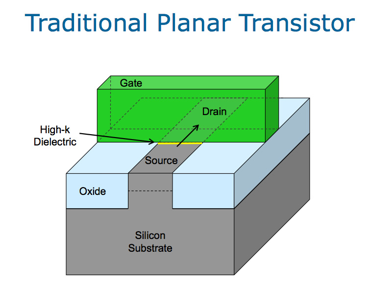
Image Courtesy Intel Corporation
I spent a couple of semesters as a computer engineering student a few years ago studying how these things work. There's a lot of math and it's not fun to do over and over again so we'll ignore all of that for now. The basics are thankfully much more fun to understand.
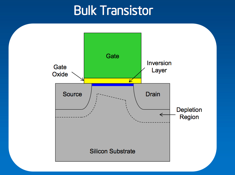
Image Courtesy Intel Corporation
The goal of a transistor is to act as a very high speed electrical switch. When on, current flows from the transistor's source to the drain. When off, current stops. The inversion layer (blue line above) is where the current flow actually happens.
Ideally a transistor needs to do three things:
1) Allow as much current to flow when it's on (active current)
2) Allow as little current to flow when it's off (leakage current)
3) Switch between on and off states as quickly as possible (performance)
The first item impacts how much power your CPU uses when it's actively doing work, the second impacts how much power it draws when idle and the third influences clock speed.
In conventional planar transistors it turns out that voltage in the silicon substrate impacts leakage current in a negative way. Fully depleted SOI (silicon on insulator) is an option to combating this effect.
The smaller you make the transistors, the more difficult it is to make advancements in all three of these areas all while increasing transistor density. After all not only do you have to worry about keeping power under control, but the whole point to shrinking transistor dimensions is to cram more of them into the same physical die area, thus paving the way for better performance (more cores, larger caches, higher performance structures, more integration).
The 3D Tri-Gate Transistor
A 3D Tri-Gate transistor looks a lot like the planar transistor but with one fundamental change. Instead of having a planar inversion layer (where electrical current actually flows), Intel's 3D Tri-Gate transistor creates a three-sided silicon fin that the gate wraps around, creating an inversion layer with a much larger surface area.
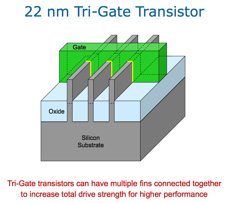
Image Courtesy Intel Corporation
There are five outcomes of this move:
1) The gate now exerts far more control over the flow of current through the transistor.
2) Silicon substrate voltage no longer impacts current when the transistor is off.
3) Thanks to larger inversion layer area, more current can flow when the transistor is on.
4) Transistor density isn't negatively impacted.
5) You can vary the number of fins to increase drive strength and performance.
The first two points in the list result in lower leakage current. When Intel's 22nm 3D Tri-Gate transistors are off, they'll burn less power than a hypothetical planar 22nm process.
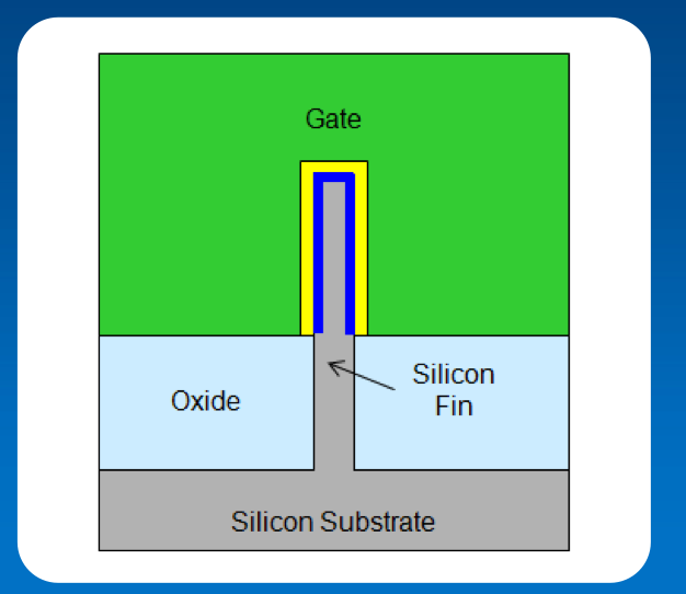
Image Courtesy Intel Corporation
The third point is particularly exciting because it allows for better transistor performance as well as lower overall power. The benefits are staggering:
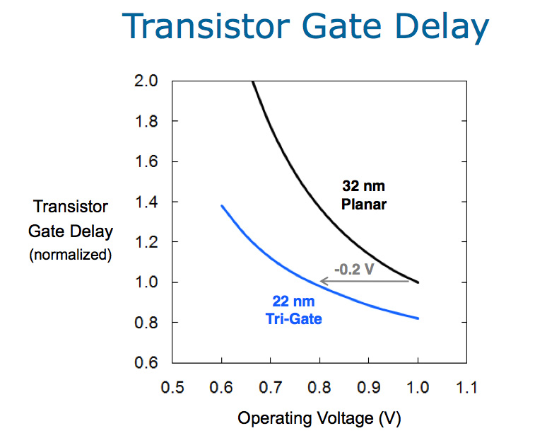
Image Courtesy Intel Corporation
At the same switching speed, Intel's 22nm 3D Tri-Gate transistors can run at 75 - 80% of the operating voltage of Intel's 32nm transistors. This results in lower active power at the same frequency, or the same active power at a higher performance level. Intel claims that the reduction in active power can be more than 50% compared to its 32nm process.

Image Courtesy Intel Corporation
At lower voltages Intel is claiming a 37% increase in performance vs. its 32nm process and an 18% increase in performance at 1V. High end desktop and mobile parts fall into the latter category. Ivy Bridge is likely to see gains on the order of 18% vs. Sandy Bridge, however Intel may put those gains to use by reducing overall power consumption of the chip as well as pushing for higher frequencies. The other end of that curve is really for the ultra mobile chips, this should mean big news for the 22nm Atom which I'm guessing we'll see around 2013.
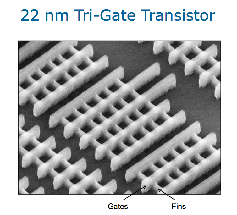
Image Courtesy Intel Corporation
You'll note that the move to 3D Tri-Gate transistors doesn't negatively impact transistor density. In fact Intel is claiming a 2x density improvement from 32nm to 22nm (you can fit roughly twice as many transistors in the same die area at 22nm as you could on Intel's 32nm process).
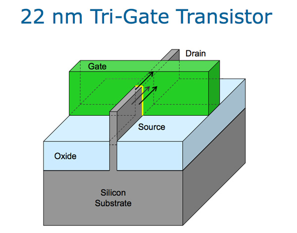
Image Courtesy Intel Corporation
It's also possible to vary the number of fins to impact drive strength and performance, allowing Intel to more finely tune/target its 22nm process to various products.
The impact on manufacturing cost is also minimal. Compared to a hypothetical Intel 22nm planar process, the 3D Tri-Gate process should only cost another 2 - 3%
Image Courtesy Intel Corporation
All 22nm products from Intel will use its 3D Tri-Gate transistors.
What Does This Mean
Intel's Ivy Bridge is currently scheduled for a debut in the first half of 2012. Intel is purposefully being vague about the release quarter as Sandy Bridge is doing well and isn't facing much competition at the high end at least.
The impact of Intel's 22nm 3D Tri-Gate transistors on high end x86 CPUs will be significant. Intel isn't expecting its competitors to move to a similar technology until 14nm. The increases in switching speed at the same voltage could allow Intel to finally hit or exceed that magical 4GHz barrier in a stock CPU. I suspect Intel will likely use the gains to deliver lower power CPUs however there's always the possibility of some very fast Extreme Edition parts.
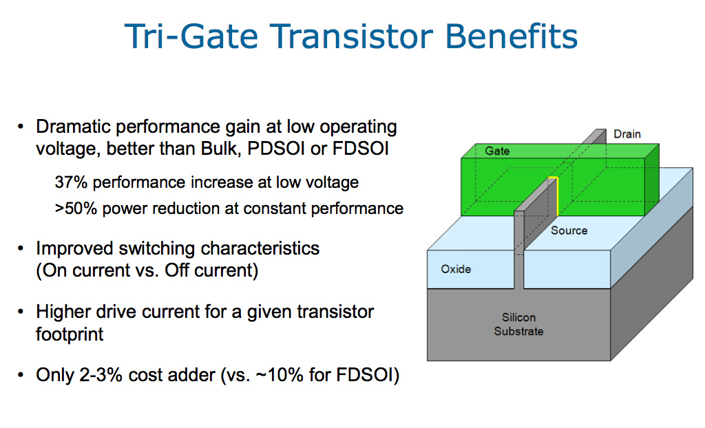
Image Courtesy Intel Corporation.
The bigger story here actually has to do with Atom. The biggest gains Intel is showing are at very low voltages, exactly what will benefit ultra mobile SoCs. Atom has had a tough time getting into smartphones and while we may see limited success at 32nm, the real future is what happens at 22nm. Atom is due for a new microprocessor architecture in 2012, if Intel goes the risky route and combines it with its 22nm process it could have a knockout on its hands.


82 Comments
View All Comments
GeorgeH - Wednesday, May 4, 2011 - link
Isn't Intel the only one with the ability to mass produce anything at 22nm right now? 3D sure sounds cool, and the theoretical benefits are easy to see, but how do we know that this isn't a "forced" innovation with PR-spin?By that I mean has 22nm simply gotten to the point where it's just getting too small to manufacture with reasonable reliability without effectively increasing size by expanding vertically? I know Intel is saying other manufacturers will be staying planar at 22nm, but I wonder if this news means that we can expect more than the usual number of manufacturing issues with those processes.
davepermen - Wednesday, May 4, 2011 - link
of course it's a forced innovation. forced in the sense that they needed to solve a problem.but still a great one, as it allows to continue going smaller while staying efficient at it (leakage increased for years, harming efficiency.. that one shifted this barrier quite a bit again).
it's like the hitachi (?) get perpendicular song about storing bits vertically: http://www.youtube.com/watch?v=-xPvD0Z9kz8
GeorgeH - Wednesday, May 4, 2011 - link
But solve what problem? The problem of "make better transistors" or the more general problem of "manufacture 22nm products without making GF100's engineers blush." If it's the former, fantastic. If it's the latter, it could have interesting implications for the rest of the industry as they follow Intel in making the 22nm transition.Azethoth - Thursday, May 5, 2011 - link
This solves the problem of making better transistors. Nobody cares about blushing engineers at nVidia.More generally, while Moore's law has held, certain patterns in it have not. Years ago heat became a problem to the point where the steady frequency increases just stopped and so multi-core became popular because that was a way to still make use of the extra transistors that stopped getting faster and so maintain a kind of speed increase.
This is an exciting new way to bump up a bunch of the performance characteristics that have languished for years now without much cost. Also it seems that it may scale a bit into the future with the use of more fins.
KarlWa - Monday, May 9, 2011 - link
Theres no reason to think Intel won't open it's fabs to producing non-x86 chips. There are rumours that they want to make A5 chips for Apple, and they may see some gain to getting back in to ARM design if they can use their experience and scale to make the best ARM chips around. They could build a fully-custom ARM SoC platform similar to what NVidia do.From a business perspective, it looks like a great way to add growth. It depends on how stubborn Intel is willing to be to hold on to the x86 architecture. It's been a big competitive advantage for them until now, but it doesn't look like ATOM is going to make significant headway. Apple are not going to give up the vertical structure of designing their own SoCs, and the big Android licensees are at such pressure to differentiate from each other that they are better suited to the ARM pick-n'-mix model with SoCs from a variety of manufacturers. That could eventually filter down to the PC business with Windows licensees replacing those of Android and the rumours of Apple moving Macs to It's own ARM chips also coming true.
The ARM SoC Market is big business and growing as fast (if not faster) than the already zippy smartphone Market. Intel needs to get involved before it becomes obsolete, and opening its fabs and/or entering the ARM SoC Market are the two best ideas I can think of for them to do it.
krumme - Wednesday, May 4, 2011 - link
Thanx for very good explanationOfcource the devil is in the detaiils, but the the flexibility for the product portforlio looks very interesting so far. Agree Atom 2013 is the one to look for, as its where things could change more fundamentally.
Shadowmaster625 - Wednesday, May 4, 2011 - link
The 5 watt ontario c-50 i at 22nm would scale down to well under 50 mm^2 and probably 2 watts on Intel's superior process. Anything less from intel would be a failure. Of course we know Intel will make it 1 watt and the gpu will be crippled. And no one will buy it but they wont care because they will be able to sell more $900 ivy bridge tablets.Rockworthy - Wednesday, May 4, 2011 - link
Is this 3D transistor technology going to be owned by Intel or will future ARM chips be able to use this too?Smooth2o - Wednesday, May 4, 2011 - link
It's not owned by anyone, it's shared technology, kinda. That's if you can figure out how to do it. Intel won't tell you. TSMC (ARM) will have it in 2015 or 2016, however, they are already one node late on that chart, so maybe longer....DanNeely - Thursday, May 5, 2011 - link
Intel might be able to patent some implementation details, but the basic finFET idea has been in academia for over 20 years and is unpatentable as a result.