ASUS F2A85-V Pro Review: A Look at FM2 with A85X
by Ian Cutress on October 10, 2012 11:20 AM EST- Posted in
- Motherboards
- Asus
- Trinity
- FM2
- A85X
The new release of Trinity processors on the desktop opens up a cascade of issues when it comes to choosing a new motherboard for your Trinity system. The main point of confusion comes in the face of chipsets, whereby multiple sockets and processor families can use the same chipsets and each motherboard manufacturer has a different naming scheme in order to differentiate the two. Both Intel and AMD have been guilty of this in the past, but in the past 18 months we had no real cause for concern - until now.
The Confusion
From the beginning, let us lay down a few facts on PC components. When a user buys a processor, the design of that processor and the pin layout determines the socket for that processor. Thus if I purchase an i7-3960X today, I know that it will fit into Socket 2011 based motherboards - similarly with the i5-2500K, it will fit into Socket 1155 motherboards. Out of the motherboards that have this socket, two main avenues are available to decide which model is suitable - the chipset, and the additional functionality.
With AMD and socket AM3+, we had choices of the 990FX, 990X and 970 chipsets. With Sandy Bridge there was P67, H67 and Z68 with some extra business level chipsets, and Ivy Bridge gets Z77, H77, B75 and others. The beauty of Sandy Bridge and Ivy Bridge is that all the consumer level chipsets are interchangeable and with BIOS updates, all motherboards in that space will work with both processors. I know that if I buy any Z68 motherboard I can fit either my Sandy Bridge processors or Ivy Bridge processors in them.
Trinity and the FM2 socket turn the above situation on its head, so to speak. If I went out and bought a Llano processor on an FM1 socket, I have a choice of either A55 or A75 chipsets. However, for FM2, I have a choice also of A55 or A75, alongside the newer A85X chipset. This means I cannot blindly look at the chipset just for a particular processor socket - it also means that motherboard manufacturers have to be static and clear with their naming structure to avoid confusion. But then again, each manufacturer has a different naming structure, which serves to confuse even more.
In terms of naming strategies, the major motherboard manufacturers have the following scheme:
ASUS: F2A85-V Pro - the initial F2 is for Trinity
Gigabyte: F2A85X-UP4 - the initial F2 is for Trinity
ASRock: FM2A75 Pro4 - the initial FM2 is for Trinity
MSI: FM2-A85XA-G65 - the initial FM2 is for Trinity
ECS: A85F2-A Deluxe - First chipset, then FM2 socket
Zotac: A75-ITX WiFi - No mention of FM2 (as per what was shown at Computex)
Biostar: A75MH2 - No direct mention of FM2 (again, from Computex)
So the key is to look for F2 or FM2 on most of the motherboard manufacturers. Failing this, look for the A85X chipset (such as the Biostar HiFi A85X) which should be specifically for FM2 and Trinity processors.
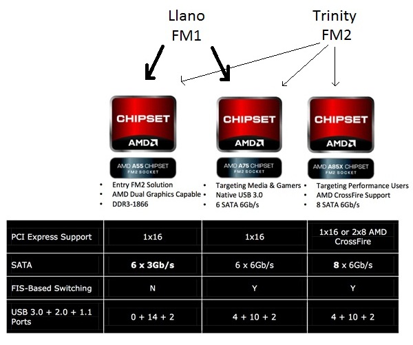
With the naming side of things out of the way, it is important we know how each chipset differs in its functionality. This is primarily summed up in the image above - the newer A85X chipset boasts eight SATA 6 Gbps ports native to the chipset. This is a key differentiator in the AMD vs. Intel battle over chipsets, with Intel only supporting two SATA 6 Gbps (and four SATA 3 Gbps) as native. Complimentary to this change, A85X also supports RAID 5, whereas A75 does not. This opens up low powered Trinity units, with onboard graphics, for use in what I would call 'typical SOHO' NAS environments - no discrete GPU with RAID 5 for redundant storage capabilities.
Also worthy of note is the graphics side of the motherboards we will be testing as part of our Trinity coverage. On A55 and A75, we are limited to a single x16 PCIe 2.0 according to the official documentation - this is despite that A75 on Llano allowed x8/x8 functionality as shown by our review of the ASRock A75 Extreme6 at launch. Whether this is a minor change for FM2 to drive users to Trinity or something else, I am not sure. However, moving to A85X does allow for a rated discrete dual x8/x8 lane allocation.
The board we are looking at today has come with a very handy chipset diagram to show exactly what is going on:
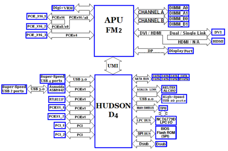
Normally on the Intel side of things, we see four lanes of PCIe 2.0 being exposed by the chipset, which would lead to x16/x4 or x8/x8/x4 lane allocations, with that final x4 lane being crippled both by the chipset routing and the bandwidth. However when it comes to Trinity, we actually have 20 PCIe 2.0 lanes coming from the APU to power PCIe devices. This gives each board using an FM2 APU the ability to do at least x16/x4 or x8/x8/x4 (with A85X) without the cripple we see with Intel. In Intel's variation, we saw Crossfire work but SLI not, due to the odd combination of SLI certification required. Chances are that if we do see SLI certification on an FM2/A85X product, then this x4 should be included, though it will be crippled if bandwidth is an issue.
One thing also to note is the lack of PCIe 3.0 functionality. AMD have had PCIe 3.0 enabled video cards for a while now, and the specification has been done and dusted for even longer. Given that the move from Llano to Trinity was an architecture jump (Stars to Piledriver modules), one would expect the shift to have occurred at this point. But for now we are still 'limited' to PCIe 2.0. I use quotation marks on the basis that for most users the jump from PCIe 2.0 to PCIe 3.0 has no influence on normal settings, but for some extreme and limited cases, PCIe 3.0 can help. There is a chance that PCIe 3.0 could be part of the new architecture, but disabled until the next family of processors are launched on FM2. Failing that, FM3 will be a more likely stomping ground for PCIe 3.0. We may have to wait until the APUs use GCN rather than VLIW-4 for their graphics cores.
With all this being said, let us move on to the first of our FM2 and Trinity reviews, with a look at the A85X chipset in the form of the ASUS F2A85-V Pro.
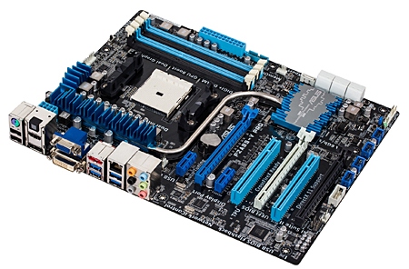
ASUS F2A85-V Pro Overview
The first review using a new processor family and a new chipset family is often difficult. The problem is multi-faceted in the sense that knowledge of a platform is often less than ideal, and the final outcome and conclusion of the board could be tainted by the processor or APU performance in comparison to previous chipsets. This is doubly compounded for this review, whereby for the first time in a long time we are dealing with a middling performance processor (in the absolute sense) in comparison to anything previous over the past 12 months. Since our last foray into this space with Llano and Zacate, our benchmark suite has changed for the most part (such as GPU testing at 2560x1440), but there are some common tests from which we can draw conclusions. Also worth noting is that the first review of a new chipset often leaves few comparison points to be made to the rest of the motherboards in that chipset, given no testing has been performed on the others.
Nevertheless, ASUS did send us the F2A85-V Pro and overall impressions with the motherboard itself are positive. Power delivery heatsinks are sufficient for the Trinity platform, but bolstered by heatpipe connections to the chipset heatsink. Despite the numerous SATA and USB ports offered by the chipset, the board offers an additional ASMedia USB 3.0 controller with the board to take advantage of UASP protocols in USB 3.0 throughput. The board also comes with ASUS Digital Power Delivery options (DIGI+) for CPU and memory, should that be of use to the user for pushing the limits of the board or keeping power consumption down.
Connectivity on the board gives us access to PS/2, USB 2.0, all four common video outputs (VGA, DVI-D, HDMI, Displayport), eSATA, USB 3.0, gigabit Ethernet and PCI connectors on board. Memory is connected via T-Topology rather than Daisy Chain, which in principle should aid in four DIMM memory overclocking. The main areas ASUS like to push with their products is the software, such as Network iControl for program priority of networking traffic, and Fan Xpert 2 which gives the user complete control of all the fan headers (five) on board through the OS including auto tuning. We also get three-way PCIe device functionality onboard, and access to ASUS' USB BIOS Flashback, which allows updating the BIOS via USB without a CPU, memory or video card connected.
Downsides are few, though I would like to know why the single sided latch system ASUS put on their Intel boards for memory is not present here. In the box I would have liked to have seen a front facing USB panel, though as time goes on we only seem to find this in products with two USB 3.0 headers on board. From a personal perspective, I enjoy having a two-digit debug in order to diagnose motherboard issues but ASUS have instead put onboard their Q-LED system which indicates where in the POST process there are issues (while nice, I do not find it fine-grained enough). In a similar ilk, there are no power/reset buttons on board, but like the two-digit debug, these have very few roles when the system is in a case and working smoothly.
Performance wise, it is hard to get past the performance of the Trinity when compared to Ivy Bridge and the like. From a practical standpoint, the lack of floating point units in the CPU gives cause for concern as not everyone codes in hex or integer style (my own personal software all uses FP – INT would be confusing to code for me for negligible gain on most architectures). As this is the first FM2 board we are testing, there are very few comparative conclusions we can draw of the board compared to the competition. We can say that ASUS are still pushing their USB 3.0 boost which gives some distinct read/write improvement numbers, but the copy times for both chipset based and controller based USB 3.0 ports are not as good as Intel offerings. One point of concern is the DPC latency, which for this product jumped around from ~100 microseconds to 600+ microseconds. Usually these jumps are attributed to monitoring software, however there was none loaded into the system. The DPC test should ideally score less than 200 microseconds, but under 500 microseconds is still a pass – for the F2A85-V Pro to score worse than 500 is a little disappointing if audio processing is the main reason to purchase this product. I suspect this could be fixed with a minor BIOS update.
Visual Inspection
I will be blunt as well as fair - in my opinion, mid range boards seem to lack a level of aesthetic finesse that we get with higher end products. Case in point, I recently fitted a new $100 micro ATX board into my brothers new machine and it was not as pretty as the equivalent high end model I had in my machine. We see something of this mid-range aesthetics on the ASUS F2A85-V Pro. This is by no means negative, but on the higher end niche products, the handling and feel of the PCB just seems cleaner and more efficient, presumably due to consolidation of some of the onboard chips through a higher budget. It is an interesting point to consider. Despite this, everything that can be brought down gratis from the higher end models will end up in the mid range (routing, BIOS, efficiency).
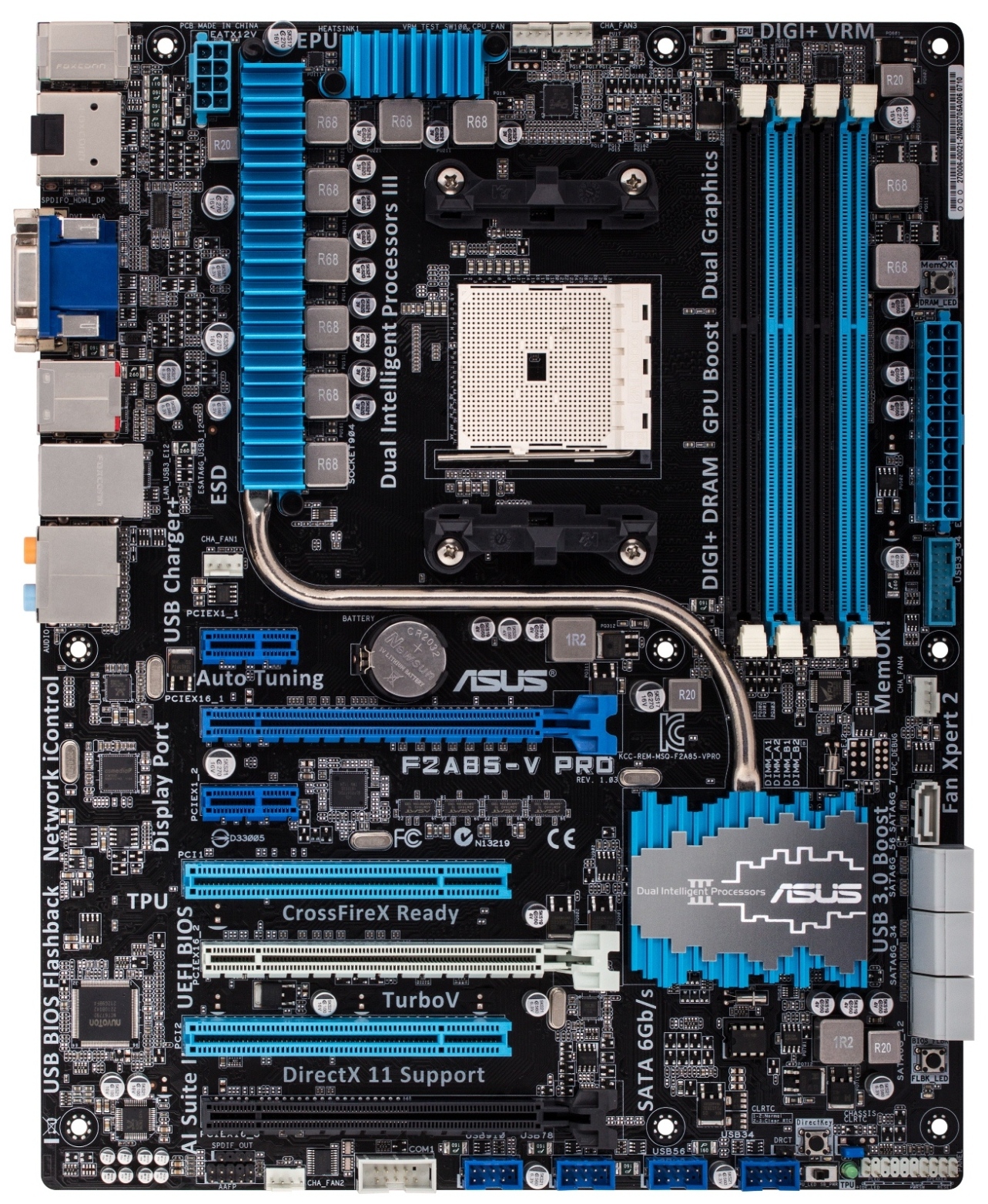
With the F2A85-V Pro we have a standard AMD sized socket for the processor, which in comparison to the competition is a large area to set aside for the processor and a hangover from AM2 requirements. As processors become more efficient, I would like to see AMD redesign the socket area for efficiency and size, which will allow motherboard manufacturers more real estate and room to innovate in the area. Nevertheless, due to the size of the power delivery heatsinks there is plenty of room for even the beefiest air coolers on this motherboard - at a stretch (without directly testing due to lack of equipment), it could be possible that Noctua NH-D14 users may be limited in memory module space with the first slot being covered.
The socket area has four fan headers within easy reach - two 4-pin headers above the socket (one CPU, one chassis), a 4-pin chassis header underneath the power delivery to the bottom left, and another 4-pin chassis header below the USB 3.0 header to the right of the board. The final 4-pin chassis header is found at the bottom of the board next to the onboard audio.
Along the right hand side, the first feature of note is the MemOK! Button - a handy device useful if you set the memory too high. I use it quite regularly when pushing the memory in conjunction with a CPU overclock. Underneath we get the 24-pin ATX power connector, a USB 3.0 header (from the chipset), a fan header, then our SATA ports. As the AMD A85X chipset allows up to eight SATA 6 Gbps ports, chances are we will only see extra SATA controllers on a motherboard if the controller affords special functionality. ASUS have decided to directly use seven ports on this side of the board, with the eighth port being the eSATA port on the IO panel. These SATA ports are capable of RAID 0, 1, 5 and 10. Following this is the BIOS Flashback button on board (rather than an IO panel button as seen on previous iterations).
The chipset heatsink covers the A85X chip, which according to specifications can consume up to 7.8 watts. With this heatsink being connected via heatpipe, the main function is to aid in the power delivery cooling, even if the heatsink design does not seem to maximize surface area.
On the bottom of the board are various ports available from use. From left to right we get the front panel audio, a 4-pin fan header, a COM header, four USB 2.0 headers, the TPU switch and then the front panel header. The PCIe layout is reasonable for a two way GPU setup with room for either a PCIe x1, PCI or PCIe x4 card. From top to bottom we get a PCIe x1, PCIe x16 (x8 in dual), x1, PCI, x8, PCI, x4.
One extra switch on the board is related a lot to the first Intel X79 board I reviewed. On that board we were given a switch on the IO panel that when activated would send the user to the BIOS on the next boot. We have a similar technology here on the F2A85-V Pro in the form of a DirectKey button above the TPU switch along the bottom. When pressed in the OS, it will shut down the system and on the next boot go straight into BIOS. When pressed if the system is off, it will start up the system and boot into the BIOS. This is highly useful for overclockers and reviewers such that we do not have to hold down the Del button on boot to access the BIOS. This is not an ASUS specific feature for FM2 and A85X as I have seen it on other products, but I reckon it is a good feature to have nonetheless, even if it seems odd to include it without having power/reset buttons or a Debug LED.
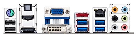
The rear IO panel gives us PS/2 functionality in a combination port, two USB 2.0 in black, optical S/PDIF output, all four VGA outputs (HDMI, DP, D-Sub, DVI-D), eSATA 6 Gbps (in red), four USB 3.0 (in blue, two from an ASMedia controller, two from chipset), gigabit Ethernet (Realtek 8111F) and audio jacks (Realtek ALC892).
Board Features
| ASUS F2A85-V Pro | |
| Price | Link |
| Size | ATX |
| CPU Interface | FM2 |
| Chipset | AMD A85X |
| Memory Slots |
Four DDR3 DIMM slots supporting up to 64 GB Dual Channel, 1066-1866MHz |
| Video Outputs |
VGA DVI-D HDMI DP |
| Onboard LAN | Realtek 8111F |
| Onboard Audio | Realtek ALC892 |
| Expansion Slots |
1 x PCIe 2.0 x16 (x8 in dual) 1 x PCIe 2.0 x8 1 x PCIe 2.0 x4 2 x PCIe 2.0 x1 2 x PCI |
| Onboard SATA/RAID |
7 x SATA 6 Gbps (FCH), RAID 0, 1, 5, 10 1 x eSATA 6 Gbps (FCH) |
| USB |
4 x USB 3.0 (FCH) [2 back panel, 2 onboard] 2 x USB 3.0 (ASMedia) [2 back panel] 10 x USB 2.0 (FCH) [2 back panel, 8 onboard] |
| Onboard |
7 x SATA 6 Gbps 1 x USB 3.0 Header 4 x USB 2.0 Headers 1 x COM Header 1 x Front Panel Audio 5 x Fan Headers 1 x MemOK! Button 1 x USB BIOS Flashback Button 1 x DirectKey Button TPU/EPU Switches Q-LED |
| Power Connectors |
1 x 24-pin ATX Power Connector 1 x 8-pin CPU Power Connector |
| Fan Headers |
1 x CPU (4-pin) 4 x CHA (4-pin) |
| IO Panel |
1 x PS/2 Combination Port 1 x VGA 1 x DVI-D 1 x HDMI 1 x DP 2 x USB 2.0 2 x USB 3.0 (Chipset) 2 x USB 3.0 (ASMedia) 1 x GbE (Realtek 8111F) 1 x Optical S/PDIF Output Audio Jacks (Realtek ALC892) ` |
| Warranty Period | 3 Years |
| Product Page | Link |
The F2A85-V Pro currently retails at launch for $140, which is around $20 more expensive than the most powerful FM2 processor. This price comparison usually means that the board should provide all the functionality a user would need. So our limitations to Realtek audio and NIC is more due to the fact this is AMD rather than Intel (Gigabyte could call on Atheros for their products), though the decision to use an ALC892 rather than the ALC898 is a little odd. Perhaps dual NIC would have been nice, or the fact that the Pro board in Z77 has the combination WiFi/Bluetooth module on board makes me wonder how much of a price increase that would have caused for a product like this.


66 Comments
View All Comments
IanCutress - Wednesday, November 28, 2012 - link
1) Interestingly enough it is not a reviewers job to debug. I do correlate my results to the manufacturers, but I test on the latest publicly available BIOS at the time of testing. If I sat around waiting for 'the next BIOS' then each review would take 3x as long and I couldn't feed my family. Sorry to disappoint. (Also, not all reviewers are masculine as per your pronoun usage.)2) The USB 3.0 and SATA 6 Gbps are both native on Intel and AMD unless specified otherwise. I believe it is an appropriate comparison. People deciding to upgrade will want a comparison between what is available now in the market, not what was on the market. There is scope for editorials to look at how certain dynamics have changed over the years, but also tests change. My old data for 9xx chipsets is not relevant here.
3) Again, tests change over time in order to correlate with newer hardware and test the capabilities. If you have the spare time to dig out the hardware and run the newer tests, that's up to you. The other 14 motherboards I have in needed to be tested get priority here otherwise they become irrelevant. I would love to have infinite hardware and infinite time to do the comparisons, but that is not a logistical possibility.
4) Each chipset is tested against a single CPU. P67/Z68 was i5-2500K, X79 was i7-3960X, FM1 was A6-3650, FM2 was A10-5800K.
5) My apologies, next time I'll forgo the initial release review because it's the only board in my hand before release and wait a few months until I have six reviewed then post them at once when they become a little irrelevant.
6) Have you? Have you got time to do stability testing? What about testing it at high altitude, or in the Sahara?
If you believe there are things missing from the review, helpfully suggest additions for future consideration. My email is through my name on the review.
brookheather - Thursday, October 11, 2012 - link
Typo - "there is few reasons to jump on board to Trinity".Mugur - Friday, October 12, 2012 - link
Well, she was hot back in the first Matrix days... :-)silverblue - Thursday, October 11, 2012 - link
"With that being said, it is clear that video conversion is an INT process and all four of the A10-5800K INT units are being used"Are they, though? If so, it's a bit disappointing. Are all four threads maxed out in Task Manager? It'd be interesting to see a 4C/4T Intel processor thrown in there (2500K seems a perfect candidate) as well.
From looking at this, it should mean that an identically clocked Piledriver (83xx) CPU wouldn't be too far behind the 3770K in this one test. It does also mean, unfortunately, that even with linear performance scaling, even the top Piledriver CPU won't dethrone Thuban in the 3DPM MP test.
Soulnibbler - Thursday, October 11, 2012 - link
What does is this line in the performance section supposed to mean?QUOTE:
From a practical standpoint, the lack of floating point units in the CPU gives cause for concern as not everyone codes in hex or integer style (my own personal software all uses FP – INT would be confusing to code for me for negligible gain on most architectures).
/QUOTE:
I'm assuming you are referring to the bulldozer/steamroller architecture with a shared FPU unit per pair of integer units. On first reading it implies (and this implication is uncontested by the bizarre contents of of the following parentheses) that there is no floating point unit on the chip. That is patently wrong as there is a rather nice FPU shared between every two integer cores.
The other interpretation is that you think it needs MORE than half an FPU per core. That is an arguable point, but then the strange text in the parentheses paints you as someone who needs much more study towards what actually happens in a program. So much of your normal computing occurs in integer space. There isn't really any sort of program I can easily think of where you don't use integer operations (even memory mapping is integer) many times in order to prepare to do a single FP operation. The counter examples are all pretty much graphics examples where we want to work on vectors. The Trinity FPU has a nice vector processor too. If you break down and look at the machine code that any of your programs use you will find that an overwhelming (much greater than 66%) of that code is integer code.
Crying OH NOES 1/2 A FPU, is not good reporting. YES the AMD chips lag the Intel chips, YES the design parameters are different. The unfounded supposition that performance difference are due to that specific portion of the architectural choice is frankly bad journalism. If you want to make claims like that you have to point to a set of benchmarks that demonstrate clearly that the 1/2 FPUs are to blame. I doubt this is the case as most analysis that I've seen points to larger memory subsystem problems as a much bigger factor.
IanCutress - Wednesday, November 28, 2012 - link
If your supposition is true, then the A10-5800K should not experienced as much of a decrease against the competition as it did do in the results.My 3DPM results clear my position on the matter:
"In the single threaded test, a lot of conclusions can be drawn from the comparison of AMD architectures. Direct comparison of Piledriver to Bulldozer (A10-5800K to FX-8150) gives a boost in single core performance of 7%, however comparing the old Stars cores of the A8-3850 at 2.9 GHz is roughly the same as the new Piledriver core at 4.2 GHz. So even with a 1.3 GHz advantage, Piledriver is only as good as Stars and less efficient in floating point results. If we compare Piledriver to Thuban, i.e. A10-5800K to X6 1100T, the Piledriver core gets stomped on by a good 25% performance. I find this quite staggering – most of the code I ever encountered as a computational chemist was floating point based, dealing with single and double precision on a regular basis. On this result, I would steer clear of Piledriver.
The multithreaded version of 3DPM is slightly tougher to analyze. Due to the FP nature of the program, the A10-5800K is essentially a 2 core FPU processor, whereas all the other comparative AMD processors have either 4 or 6 FPUs to play with. What is perhaps worth considering is that the Bulldozer processor with 4 modules scores 326.32, whereas the Piledriver processor with only 2 modules scores 203.06, which is more than half. This would mean that the Piledriver core actually achieves 20% better performance at the same frequency, despite our ST test giving Piledriver only a 7% increase. Part of this could be put down to the architecture improvements – improved scheduling for heavily threaded loads, one of the downfalls of Bulldozer but was improved in Piledriver could be the reason here."
My basis for my comments is from a computational complexity standpoint. Sure memory mapping may be an int process, but if I only do it at the beginning and end of a matrix transformation (and thereby having a total processing time less than 0.1% of the program) then it becomes insignificant.
What AMD have done is project that applications in the future which require heavy computational throughput will be driven by INT ops. The big software vendors can do this, making video conversion and ray tracing type applications enhanced by use of INT ops. But for the non-CompSci scientist who relies more on readable code but also wants a speed increase, then going all out on the INT side may not be possible, and we get limited performance due to the scheduling and the lack of pure grunt due to the gutted APU. It's a design choice AMD have to live with, and I'm not the only one who is not entirely in favor of it.
Scootiep7 - Thursday, October 11, 2012 - link
Ok, I'm trying not to break down and just buy a Llano for my HTPC build, but does anybody know how much longer it'll be till I can get some nice options for a mini-ITX such as http://news.softpedia.com/news/MSI-Presents-FM2-A7... and the 5700k? What's the holdup on these!groundhogdaze - Thursday, October 11, 2012 - link
AMD should play to their strengths which is an affordable CPU with a relatively fast integrated GPU. That means focusing a small form factor systems such as AIO, ITX, HTPC class systems, however, I am surprised and disappointed at the relative lack of options when it comes to ITX FMx motherboards. I sold my AMD stock when I concluded they had their strategy wrong. Most folks who want to use a full sized case would also want to use a dedicated GPU, otherwise, what's the point of having a full sized case? Wrong marketing choice.Unless AMD can improve their heat/power ratings, the Intel G530 makes better sense as a NAS solution as it is dirt cheap and uses less power than its advertised 65w TDP while running circles around the Atom class processors. I hope AMD is reading the forums and best luck to them.
Mugur - Friday, October 12, 2012 - link
You are right. Full ATX and Trinity makes little sense. mATX and mini ITX with 8 SATA3 and integrated graphics should be the focus. Full ATX in fact makes little sense today, anyway... :-)If you want more than a NAS from a server, the best 65W Trinity part should be nice. I have a Phenom II X2 rated 80W in my HTPC and an Athlon II X4 (95W) in my server at home. Neither of them comes even closer to their rated TDP, according to the "green" ICs and software of the motherboards (Gigabyte and Asus).
silverblue - Friday, October 12, 2012 - link
AMD seems to volt their processors conservatively, so K10Stat (or other utilities) or using the BIOS to reduce the voltage may prove useful in reducing power consumption noticably without affecting performance more than a couple of percent.Toms ran an article on this as regards Trinity, and have done so with various AMD models in the past:
http://www.tomshardware.com/reviews/a10-5800k-trin...
Saving 14W for a tiny performance deficit is more than acceptable in my eyes.
I undervolted my Phenom II X3 710 as per the following article:
http://www.tomshardware.com/reviews/processor-powe...
(though I needed to raise voltages by 0.025v to keep it 100% stable in my case)