NVIDIA Tegra K1 Preview & Architecture Analysis
by Brian Klug & Anand Lal Shimpi on January 6, 2014 6:31 AM EST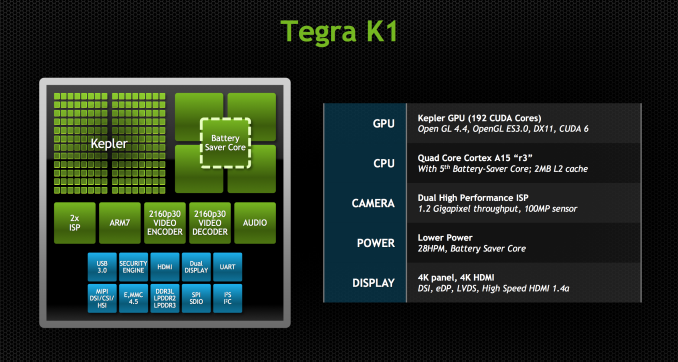
NVIDIA has taken to using CES as its platform for launching members of its Tegra mobile SoC family. This year was no different as it shifted branding a bit in its announcement of the Tegra K1, formerly known as Project Logan.
With Tegra 2 NVIDIA’s big selling point was being first to dual-core in Android. Tegra 3 attempted to do the same with being first to quad-core. Tegra 4 just made things faster. Tegra K1 on the other hand does away with the gimmicks and instead focuses on fundamentals.
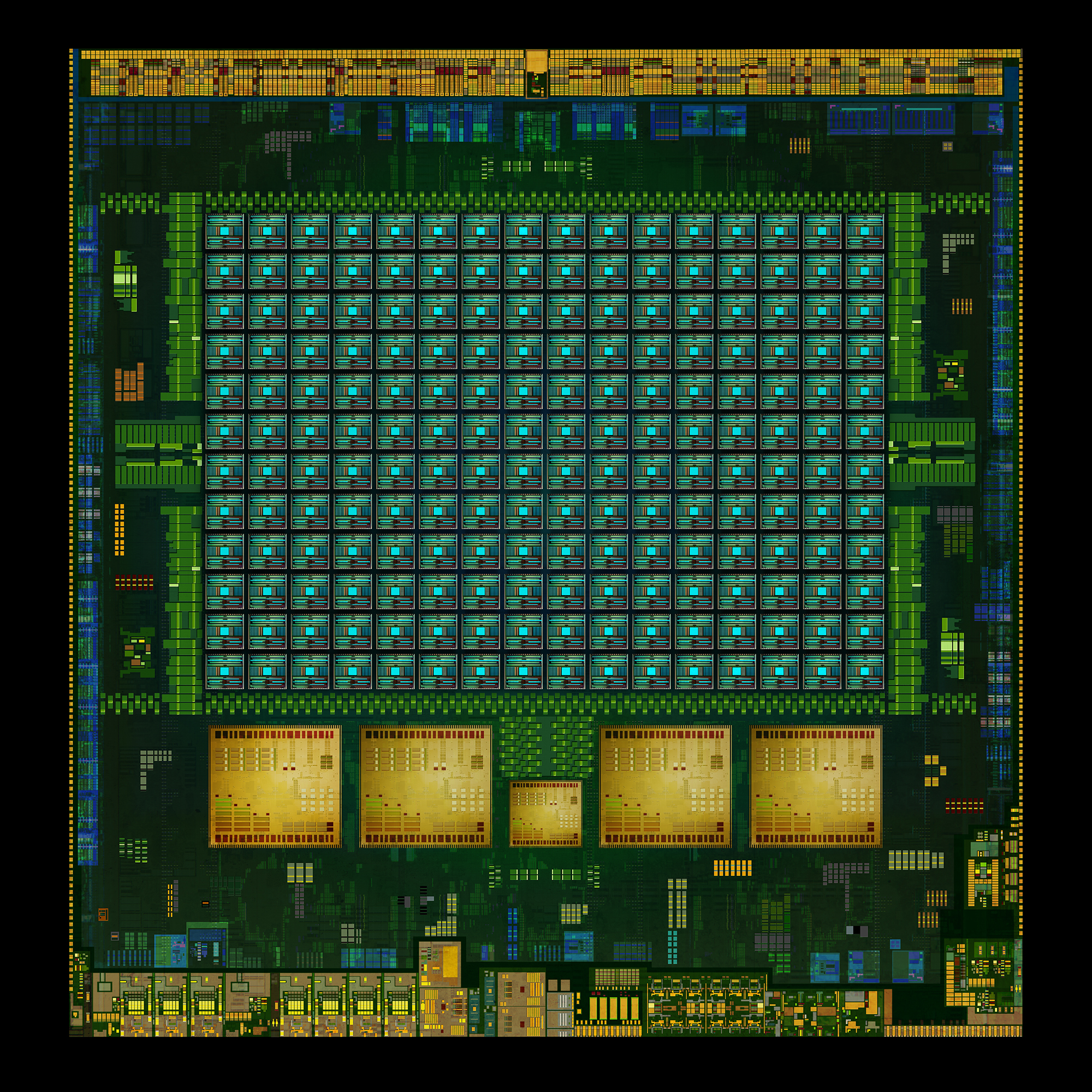
The SoC will come in two versions, one version with a quad-core (4+1) Cortex-A15, and one that leverages two of NVIDIA’s own 64-bit ARMv8 Denver CPUs. More importantly, they both ship with a full implementation of NVIDIA’s Kepler GPU architecture. In fact, Tegra K1 marks a substantial change in the way NVIDIA approaches mobile GPU design. From this point forward, all mobile GPUs will leverage the same architectures as NVIDIA’s desktop parts. As if that wasn’t enough, starting now, all future NVIDIA GeForce designs will begin first and foremost as mobile designs. NVIDIA just went from playing with mobile to dead serious in a heartbeat.
Tegra K1 will also be NVIDIA's launch vehicle for Project Denver, it's first fully custom ARMv8 CPU core. More on that in a bit.
CPU Option 1: Quad-Core ARM Cortex A15
Tegra K1 will ship in two configurations. The first went into production at the end of December 2013, is shipping to OEMs this quarter and will be in devices, allegedly, in the first half of 2014. This first configuration is based on ARM’s Cortex A15 CPU core.
Much like Tegra 4, the A15 version of Tegra K1 features four Cortex A15s synthesized for high frequencies and a fifth Cortex A15 that’s optimized for low power/frequency operation. The fifth core, what NVIDIA likes to call a shadow or companion core, is swapped in during periods of very low CPU usage (e.g. idle, screen off in your pocket updating new tweets/emails). As CPU demands grow the companion core is switched out for one of the four high performance cores, then two, then three and finally all four can be plugged in at once (but never five).
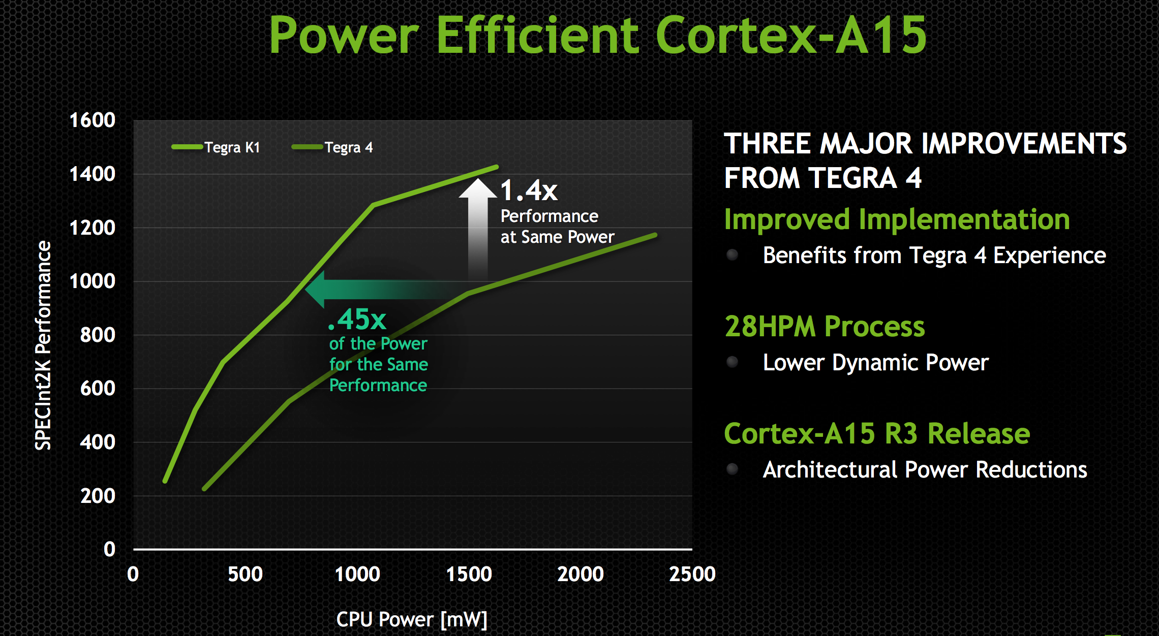
Tegra K1 ships with a newer revision of the Cortex A15 (r3p3) than what was in Tegra 4 (r2p1). ARM continuously updates its processor IP, with each revision bringing bug fixes and sometimes performance improvements. In the case of Tegra K1’s A15s, the main improvements here have to do with increasing power efficiency. With r3p0 (which r3p3 inherits) ARM added more fine grained clock gating, which should directly impact power efficiency.
The combination of the newer Cortex A15 revision and the move to 28nm HPM give Tegra K1 better performance at the same power consumption or lower power consumption at the same performance level. The reality tends to be that mobile OEMs will pursue max performance and not optimize for a good performance/power balance, but it’s at least possible to do better with Tegra K1 than with Tegra 4.
The max CPU clock goes up from 1.9GHz to 2.3GHz, a direct result of the move to 28nm HPM; 2.3GHz is the max CPU clock regardless of the number of active cores. The max performance increase over Tegra 4 running at max clocks will be just over 20%.
NVIDIA hasn’t made any changes to the L1/L2 cache configuration with Tegra K1. We’re still dealing with a shared 2MB L2 and 32KB/32KB L1s (I$+D$) per core.
The companion core can scale up to 1GHz, but tends to run at around 500MHz.
Feeding the CPU (and GPU) cores is a 64-bit wide LPDDR3 memory interface. NVIDIA will offer Tegra K1 in PoP, discrete and another package revision for standard clamshell notebook use.


88 Comments
View All Comments
da_asmodai - Monday, January 6, 2014 - link
This articles says first, first, first for Kepler core in mobile but it's not out yet and I believe everything that's claimed as a first in this article is also supported by the Adreno 420 in the already announced Snapdragon 805. I'd like to see a side by side spec comparison of Kepler, Adreno 420, and PowerVR Series 6XT.dwforbes - Monday, January 6, 2014 - link
"FP64 support is also present, at 1/24 the FP32 rate"Should this 1/2 the FP32 rate, or is it really so crippled?
Ryan Smith - Monday, January 6, 2014 - link
No, 1/24 is correct. It's so that you have native FP64 when you need it, but you aren't wasting die space on precision you aren't going to use.ddriver - Monday, January 6, 2014 - link
nvidia being cheap once again, deliberately ruining compute performance like they did with desktop GPUs for years. And let me guess, no openCL support either? Thanks but no thanks, gonna stick to qualcomm and samsung mobile platforms and amd/radeon on the desktop. And for what? To push their ridiculously and shamelessly overpriced "professional" products?GTX 780 DP @ 1/24 SP
R9 290 DP @ 1/8 SP
R9 280 DP @ 1/4 SP
Loki726 - Monday, January 6, 2014 - link
Adding big double precision units has real area and power costs (you typically can't rail gate off individual functional units). If you put full-rate double precision units in a mobile SoC it would just sit there draining your battery life.ddriver - Monday, January 6, 2014 - link
Unfortunately, power efficiency is just the excuse to deliberately cripple compute performance of consumer products. As you see, AMD has no problem providing DP support with lower penalty, which is the reason my compute farm runs radeons exclusively, because the performance per $ ratio completely destroys prosumer products. I do realize I am a very specific and narrow case, since I couldn't care less about gaming and graphics performance, since I use it only to rasterize the compute output, but still... why not go for a more performing design, considering it is not that much about efficiency but the greed for the fat profit margins of teslas and quadros that motivates nvidia to cripple DP performance to such a horrendous extent.Loki726 - Monday, January 6, 2014 - link
AMD doesn't release a mobile GPU part, and the Qualcomm parts which are based off of the old AMD VLIW5 design that they bought from AMD don't include double precision. Every little bit of power matters in mobile.ddriver - Monday, January 6, 2014 - link
The 1/24 DP performance does not come as a mobile-dedicated design, even the GTX 780 is crippled this way, even though it is an enthusiast part, where power efficiency is the least concern.Loki726 - Monday, January 6, 2014 - link
They are different strategies. Neither one is ideal for everyone.Putting double precision hardware into consumer parts is effectively asking
gamers to pay for extra area and power. I do agree that this is less of an
issue in desktop parts compared to mobile, but it is still an issue and GPUs
have enough ALUs in them that you would notice it if every one of them got 10%
less efficient in benchmarks.
AMD builds one chip and sells it into both compute and graphics markets. In
order to make it appealing for compute applications they add double precision.
They make gamers pay for this even though they never use it, but they don't have
to pay the design costs of building multiple chips. NVIDIA builds two
different designs. One chip for compute and another one for graphics (although
this round they also sold the compute chip into the graphics market - Titan).
Presumably they do this because they think that they can recoup the extra cost
of building a different chip that only compute users buy, and by doing so
they don't make gamers pay extra for double precision.
The compute chip has extra features like more registers, ECC, more double
precision units, dynamic parallelism, etc. Chip design is expensive. Think
hundreds of millions of dollars for a new design. If there were just as many
users of compute GPUs as there are gamers who buy graphics cards, the prices
would probably come down a lot.
I'm with you that I would like to have cheaper compute parts with full double
precision support, but I think the only real way to drive down chip prices is to
make them a commodity. It won't happen until there is a killer compute app
that makes every desktop owner want to go out and buy a compute GPU.
ddriver - Tuesday, January 7, 2014 - link
And how do consumers exactly "pay extra" for the better DP performance when AMD GPUs are overall much better value than nvidia gpus? It seems to me that if the extra cost is as high as you believe it is (which it really isn't) then it is AMD that pays it with its profit margins.