NVIDIA Tegra K1 Preview & Architecture Analysis
by Brian Klug & Anand Lal Shimpi on January 6, 2014 6:31 AM EST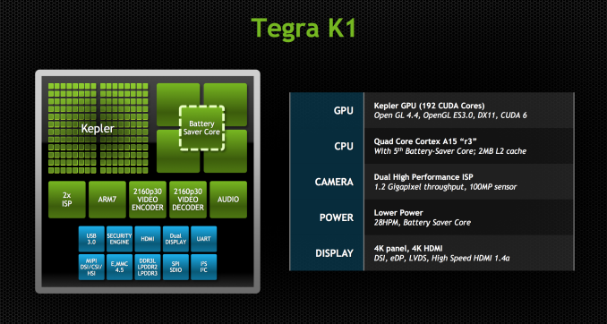
NVIDIA has taken to using CES as its platform for launching members of its Tegra mobile SoC family. This year was no different as it shifted branding a bit in its announcement of the Tegra K1, formerly known as Project Logan.
With Tegra 2 NVIDIA’s big selling point was being first to dual-core in Android. Tegra 3 attempted to do the same with being first to quad-core. Tegra 4 just made things faster. Tegra K1 on the other hand does away with the gimmicks and instead focuses on fundamentals.
The SoC will come in two versions, one version with a quad-core (4+1) Cortex-A15, and one that leverages two of NVIDIA’s own 64-bit ARMv8 Denver CPUs. More importantly, they both ship with a full implementation of NVIDIA’s Kepler GPU architecture. In fact, Tegra K1 marks a substantial change in the way NVIDIA approaches mobile GPU design. From this point forward, all mobile GPUs will leverage the same architectures as NVIDIA’s desktop parts. As if that wasn’t enough, starting now, all future NVIDIA GeForce designs will begin first and foremost as mobile designs. NVIDIA just went from playing with mobile to dead serious in a heartbeat.
Tegra K1 will also be NVIDIA's launch vehicle for Project Denver, it's first fully custom ARMv8 CPU core. More on that in a bit.
CPU Option 1: Quad-Core ARM Cortex A15
Tegra K1 will ship in two configurations. The first went into production at the end of December 2013, is shipping to OEMs this quarter and will be in devices, allegedly, in the first half of 2014. This first configuration is based on ARM’s Cortex A15 CPU core.
Much like Tegra 4, the A15 version of Tegra K1 features four Cortex A15s synthesized for high frequencies and a fifth Cortex A15 that’s optimized for low power/frequency operation. The fifth core, what NVIDIA likes to call a shadow or companion core, is swapped in during periods of very low CPU usage (e.g. idle, screen off in your pocket updating new tweets/emails). As CPU demands grow the companion core is switched out for one of the four high performance cores, then two, then three and finally all four can be plugged in at once (but never five).
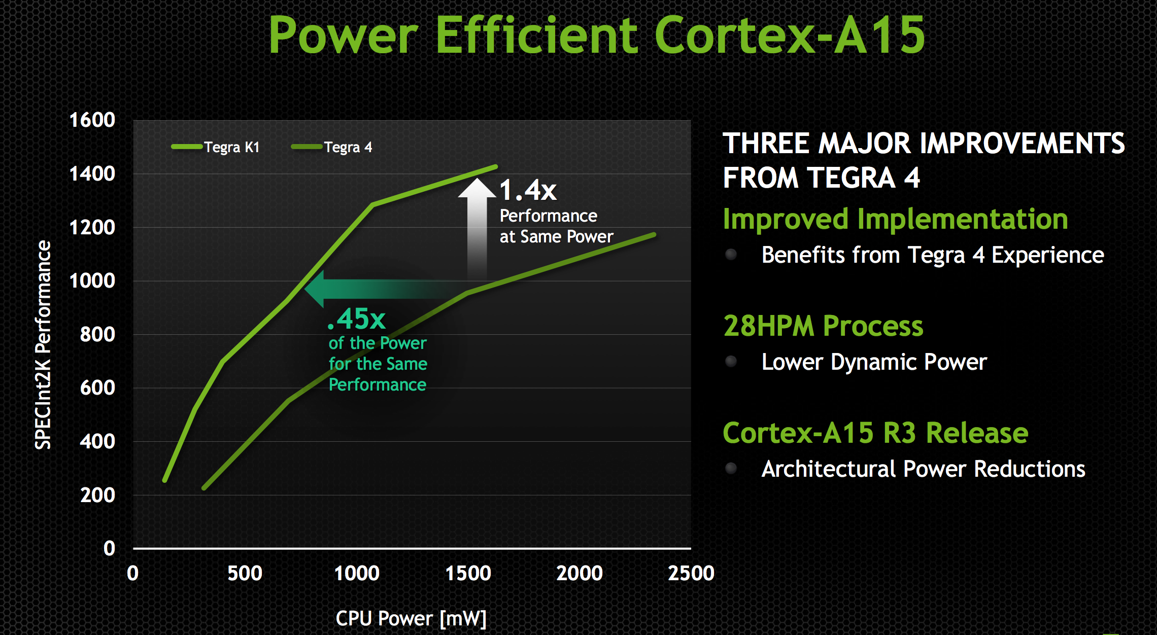
Tegra K1 ships with a newer revision of the Cortex A15 (r3p3) than what was in Tegra 4 (r2p1). ARM continuously updates its processor IP, with each revision bringing bug fixes and sometimes performance improvements. In the case of Tegra K1’s A15s, the main improvements here have to do with increasing power efficiency. With r3p0 (which r3p3 inherits) ARM added more fine grained clock gating, which should directly impact power efficiency.
The combination of the newer Cortex A15 revision and the move to 28nm HPM give Tegra K1 better performance at the same power consumption or lower power consumption at the same performance level. The reality tends to be that mobile OEMs will pursue max performance and not optimize for a good performance/power balance, but it’s at least possible to do better with Tegra K1 than with Tegra 4.
The max CPU clock goes up from 1.9GHz to 2.3GHz, a direct result of the move to 28nm HPM; 2.3GHz is the max CPU clock regardless of the number of active cores. The max performance increase over Tegra 4 running at max clocks will be just over 20%.
NVIDIA hasn’t made any changes to the L1/L2 cache configuration with Tegra K1. We’re still dealing with a shared 2MB L2 and 32KB/32KB L1s (I$+D$) per core.
The companion core can scale up to 1GHz, but tends to run at around 500MHz.
Feeding the CPU (and GPU) cores is a 64-bit wide LPDDR3 memory interface. NVIDIA will offer Tegra K1 in PoP, discrete and another package revision for standard clamshell notebook use.


88 Comments
View All Comments
jerrylzy - Tuesday, January 7, 2014 - link
Exactly. I don't see Loki726's point of gamers paying extra $ for Double Precision. AMD Cards are generally much cheaper at the same performance level, though at the cost of power consumption.Loki726 - Tuesday, January 7, 2014 - link
I mean compared to a world where AMD decided to rip out the double precision units. There are obviously many (thousands) other factors that do into the efficiency of a GPU.jerrylzy - Tuesday, January 7, 2014 - link
Unfortunately, instead of using VLIW 5, Qualcomm implemented new scalar architecture way back in adreno 320.Loki726 - Tuesday, January 7, 2014 - link
Yep, the have improved on it, but they started with the AMD design. My point was that the Qualcomm GPU is a better comparison point to a Tegra SoC than an AMD desktop part.ddriver - Wednesday, January 8, 2014 - link
The decision to chose Qualcomm in favor of Tegra would be based entirely on the absence of OpenCL support in Tegra. Exclusive cuda? Come on, who would want to invest into writing a parallel accelerated high performance routine that only works on like no more than 5% of the hardware-capable to run it devices? Not me anyway.The mention of the radeon was regarding a completely different point - that nvidia sacks DP performance even where it makes no sense to, and is IMO criminal to do so - the "gain" of such a terrible DP implementation is completely diminished by the loss of potential performance and possibility of accelerating a lot of professional workstation software. And for what, so the only spared parts - the "professional" products can have their ridiculous prices better "justified"? Because it is such a sweet deal to make a product 10% more expensive to make and ask 5000% more money for it.
Which is the reason AMD offers so much more value, while limp and non-competitive in the CPU performance, the place where computation is really needed - professional workstation software can greatly benefit from parallelization, and the much cheaper desktop enthusiast product actually delivers more raw computational power than the identical, but more conservatively clocked fireGL analog. Surely, fireGL still has its perks - ECC, double the memory, but those advantages shine in very rare circumstances, in most of the professional computation demanding software the desktop part is still an incredibly lucrative investment, something you just don't get with nvidia because of what they decided to do the last few years, coincidentally the move to cripple DP performance to 1/24 coincided with the re-pimping of the quadros into the tesla line. I think it is rather obvious that nvidia decided to shamelessly milk the parallel supercomputing professional market, something that will backfire in their face, especially stacking with the downplay-ment of OpenCL in favor of a vendor exclusive API to use the hardware.
Loki726 - Wednesday, January 8, 2014 - link
Agreed with the point about code portability, but that's an entirely different issue. I'd actually take the point further and say that OpenCL is too vendor specific -> it only runs on a few GPUs and has shaky support on mobile. Parallel code should be a library like pthreads, C++ (or pick your favorite language) standard library threads, or MPI. Why program in a new language that is effectively C/C++, except that it isn't?I personally think that if a company artificially inflates the price of specific features like double precision, then they leave themselves open to being undercut by a competitor and they will either be forced to change it or go out of business. As I said, AMD's design choice penalizes gamers, but helps users who want compute features, and NVIDIA's choice benefits gamers, but penalizes desktop users who want the best value for some compute features like double precision.
I have a good understanding of circuit design and VLSI implementation of floating point units and I can say that the area and power overheads of adding in 768 extra double precision units to a Kepler GPU or 896 double precision units to a GCN GPU would be noticeable, even if you merged pairs of single precision units together and shared common logic (which would create scheduling hazards at the uArch level that could further eat into perf, and increase timing pressure during layout).
Take a look at this paper from Mark Horowitz (an expert) that explores power and area tradeoffs in floating point unit design if you don't believe me. It should be easy to verify. http://www.cpe.virginia.edu/grads/pdfs/August2012/... . Look at the area and power comparisons in Table 1, scale them to 28nm, and multiply them by ~1000x (to get up to 1/2 or 1/4 of single precision throughput).
Double precision units are big, and adding a lot of them adds a lot of power and area.
Krysto - Saturday, January 11, 2014 - link
I want to believe OpenCL was left out because they've been trying to squeeze so much in this time-frame already. But since they fully ported everything in one swoop, I still find it hard to believe they didn't omit it on purpose. Hopefully, they'll support OpenCL 2.0 in Maxwell, because OpenCL 2.0 also offers some great parallelism features, which Maxwell could take advantage of.Andromeduck - Wednesday, January 8, 2014 - link
Isn't that what the GTX Titan is for?Jon Tseng - Monday, January 6, 2014 - link
Sounds very interesting. The Q for me though as you allude to at the end is whether they can recruit devs to utilise this. Especially when mobile games are a freemium dominated world the temptation is to code for lowest common denominator/max audience, probably with a Samsung label on it (I'm not complaining - its whats enabled me to run World of Tanks happily on my Bay Trail T100!).World beating GPU tech no use unless people are utilising it. Interesting thought about getting MSFT on board though - I guess the downer is that Windows Phone is a minority sport still, and tablet wise it would have to be Windows RT... :-x
nicolapeluchetti - Monday, January 6, 2014 - link
The processing power might be the same as the X-Box 360-PS 3 but using Direct X doesn't incur in a performance Hit?