AMD’s Kaveri: Pre-Launch Information
by Ian Cutress on January 6, 2014 8:00 PM EST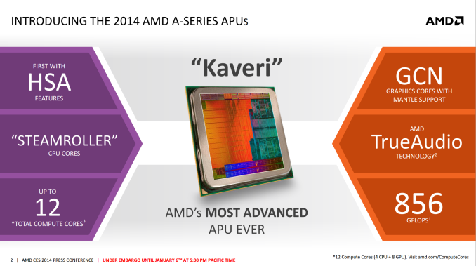
On the back of AMD’s Tech Day at CES 2014, all of which was under NDA until the launch of Kaveri, AMD have supplied us with some information that we can talk about today. For those not following the AMD roadmap, Kaveri is the natural progression of the AMD A-Series APU line, from Llano, Trinity to Richland and now Kaveri. At the heart of the AMD APU design is the combination of CPU cores (‘Bulldozer’, ‘Steamroller’) and a large dollop of GPU cores for on-chip graphics prowess.
Kaveri is that next iteration in line which uses an updated FM2+ socket from Richland and the architecture is updated for Q1 2014. AMD are attacking with Kaveri on four fronts:
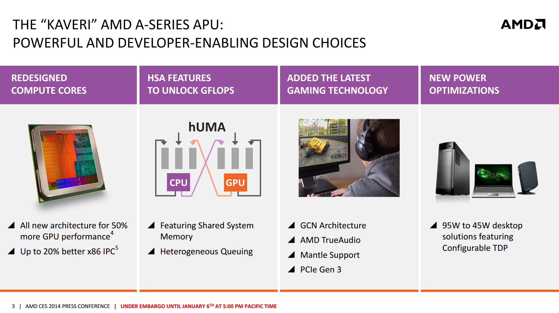
Redesigned Compute Cores* (Compute = CPU + GPU)
Kaveri uses an enhanced version of the Richland CPU core, codename Steamroller. As with every new CPU generation or architecture update, the main goal is better performance and lower power – preferably both. AMD is quoting a 20% better x86 IPC with Kaveri compared to Richland when put clock to clock. For the purposes of this information release, we were provided with several AMD benchmarking results to share:
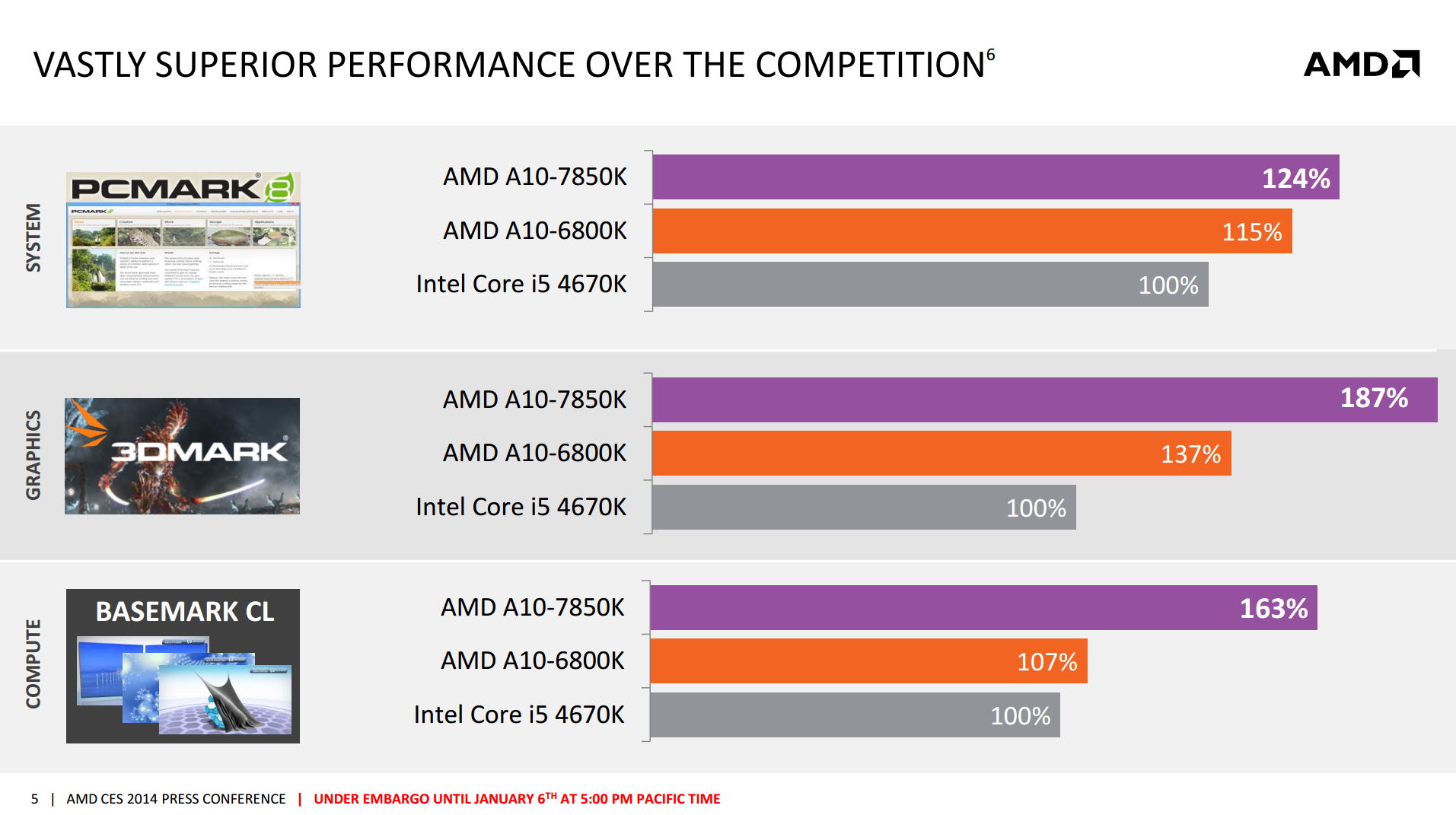
These results border pretty much on the synthetic – AMD did not give any real world examples today but numbers will come through in time. AMD is set to release two CPUs on January 14th (date provided in our pre-release slide deck), namely the A10-7700K and the A10-7850K. Some of the specifications were also provided:
| AMD APUs | ||||
|
Richland A8-6600K |
Richland A10-6800K |
Kaveri A10-7700K |
Kaveri A10-7850K |
|
| Release | June 4 '13 | June 4 '13 | Jan 14th '14 | Jan 14th '14 |
| Frequency | 3900 MHz | 4100 MHz | ? | 3700 MHz |
| Turbo | 4200 MHz | 4400 MHz | ? | ? |
| DRAM | DDR3-1866 | DDR3-2133 | DDR3-2133 | DDR3-2133 |
| Microarhitecture | Piledriver | Piledriver | Steamroller | Steamroller |
| Manufacturing Process | 32nm | 32nm | ? | ? |
| Modules | 2 | 2 | ? | 2 |
| Threads | 4 | 4 | ? | 4 |
| Socket | FM2 | FM2 | FM2+ | FM2+ |
| L1 Cache |
2 x 64 KB I$ 4 x 16 KB D$ |
2 x 64 KB I$ 4 x 16 KB D$ |
? | ? |
| L2 Cache | 2 x 2 MB | 2 x 2 MB | ? | ? |
| Integrated GPU | HD 8570D | HD 8670D | R7 | R7 |
| IGP Cores | 256 | 384 | ? | 512 |
| IGP Architecture | Cayman | Cayman | GCN | GCN |
| IGP Frequency | 844 | 844 | ? | 720 |
| Power | 100W | 100W | ? | 95W |
All the values marked ‘?’ have not been confirmed at this point, although it is interesting to see that the CPU MHz has decreased from Richland. A lot of the APU die goes to that integrated GPU, which as we can see above becomes fully GCN, rather than the Cayman derived Richland APUs. This comes with a core bump as well, seeing 512 GPU cores on the high end module – this equates to 8 CUs on die and what AMD calls ’12 Compute Cores’ overall. These GCN cores are primed and AMD Mantle ready, suggesting that performance gains could be had directly from Mantle enabled titles.
Described in AMD’s own words: ‘A compute core is an HSA-enabled hardware block that is programmable (CPU, GPU or other processing element), capable of running at least one process in its own context and virtual memory space, independently from other cores. A GPU Core is a GCN-based hardware block containing a dedicated scheduler that feeds four 16-wide SIMD vector processors, a scalar processor, local data registers and data share memory, a branch & message processor, 16 texture fetch or load/store units, four texture filter units, and a texture cache. A GPU Core can independently execute work-groups consisting of 64 work items in parallel.’ This suggests that if we were to run asynchronous kernels on the AMD APU, we could technically run twelve on the high end APU, given that each Compute Core is capable of running at least one process in its own context and virtual memory space independent of the others.
The reason why AMD calls them Compute Cores is based on their second of their four pronged attack: hUMA.
HSA, hUMA, and all that jazz
AMD went for the heterogeneous system architecture early on to exploit the fact that many compute intensive tasks can be offloaded to parts of the CPU that are designed to run them faster or at low power. By combining CPU and GPU on a single die, the system should be able to shift work around to complete the process quicker. When this was first envisaged, AMD had two issues: lack of software out in the public domain to take advantage (as is any new computing paradigm) and restrictive OS support. Now that Windows 8 is built to allow HSA to take advantage of this, all that leaves is the programming. However AMD have gone one step further with hUMA, and giving the system access to all the memory, all of the time, from any location:
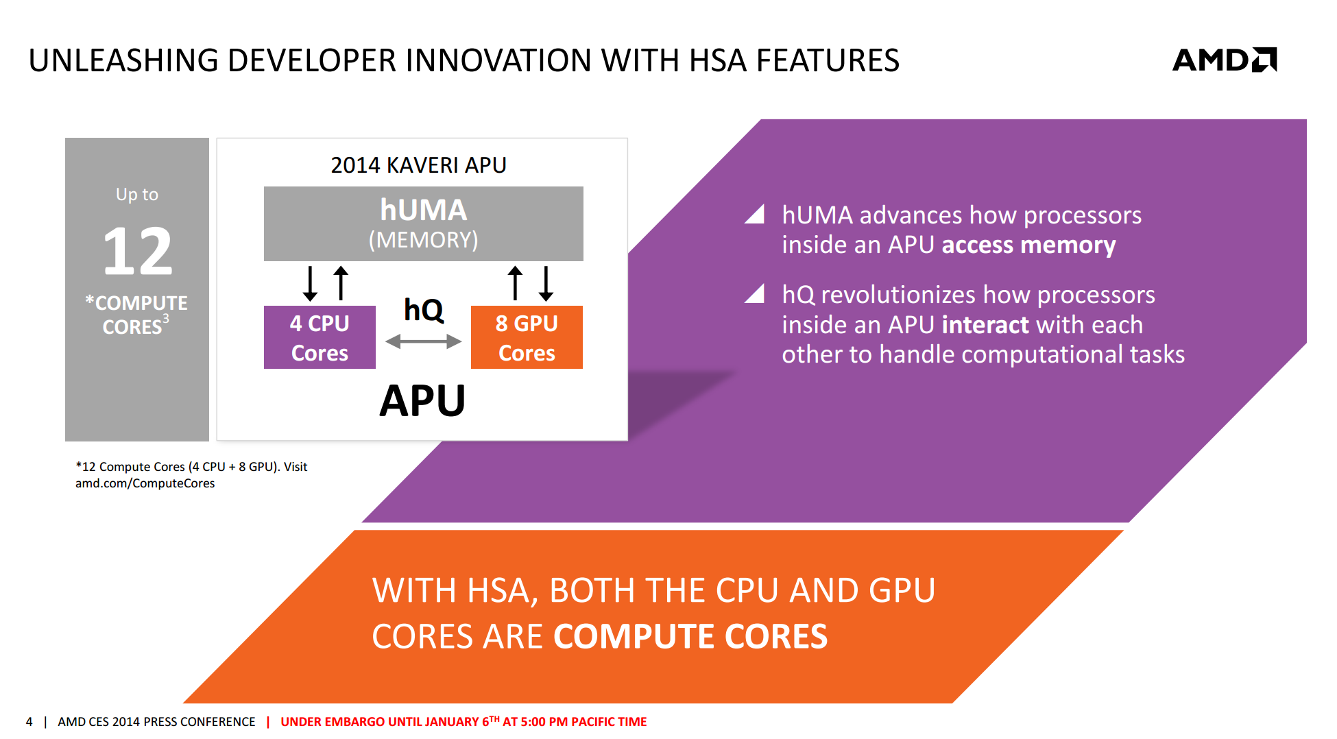
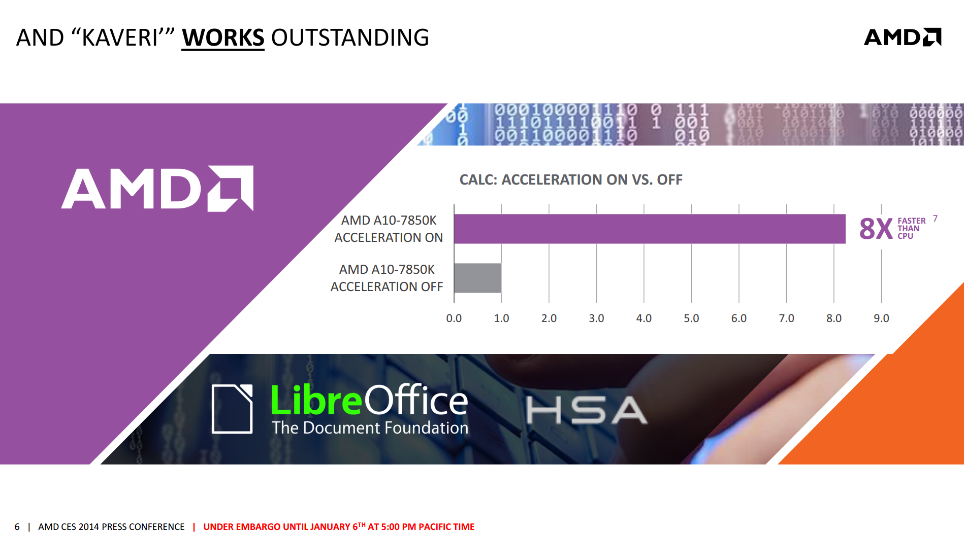
Now that Kaveri offers a proper HSA stack, and can call upon 12 compute cores to do work, applications that are designed (or have code paths) to take advantage of this should emerge. One such example that AMD are willing to share today is stock calculation using LibreOffice's Calc application – calculating the BETA (return) of 21 fake stocks and plotting 100 points on a graph of each stock. With HSA acceleration on, the system performed the task in 0.12 seconds, compared to 0.99 seconds when turned off.
Prong 3: Gaming Technologies
In a year where new gaming technologies are at the forefront of design, along with gaming power, AMD are tackling the issue on one front with Kaveri. By giving it a GCN graphics backbone, features from the main GPU line can fully integrate (with HSA) into the APU. As we have seen in previous AMD releases and talks, this means several things:
- Mantle
- AMD TrueAudio
- PCIe Gen 3
AMD is wanting to revolutionize the way that games are played and shown with Mantle – it is a small shame that the Mantle release was delayed and that AMD did not provide any numbers to share with us today. The results should find their way online after release however.
Prong 4: Power Optimisations
With Richland we had CPUs in the range of 65W to 100W, and using the architecture in the FX range produced CPUs up to 220W. Techincally we had 45W Richland APUs launch, but to date I have not seen one for sale. However this time around, AMD are focusing a slightly lower power segment – 45W to 95W. Chances are the top end APUs (A10-7850K) will be 95W, suggesting that we have a combination of a 20% IPC improvement, 400 MHz decrease but a 5% TDP decrease for the high end chip. Bundle in some HSA and let’s get this thing on the road.
Release Date
AMD have given us the release date for the APUs: January 14th will see the launch of the A10-7850K and the A10-7700K. Certain system builders should be offering pre-built systems based on these APUs from today as well.


133 Comments
View All Comments
jdietz - Wednesday, January 8, 2014 - link
AMD has the right idea allocating most of the die to the GPU. Intel would destroy AMD if they did the same. Any ideas as to why Intel doesn't allocate more of their dies to the GPU?UtilityMax - Wednesday, January 8, 2014 - link
Probably because most users and hardware vendors don't care. A bulk of enterprise PC users don't care for playing games or running multimedia apps either on desktops or laptops. Likewise, a lot of people don't play games on PCs these days. Those who do play on PCs are split into groups, those who buy a separate video card and those who don't. So IMO, so far the APU user market is still kind of small. AMD is hyping it and hoping that APUs will take off big time. After all, AMD probably has an advantage over Intel in the GPU area. Although, I suspect Intel will be able to respond to AMD if they really have to.abufrejoval - Thursday, January 9, 2014 - link
You can't do 1080p or better out of DDR3, no matter how much die space you give to the GPU: It's not a GPU limitation but a bandwidth issue. That's the whole problem with the APUs, too.Of course once you were to put the entire GPU DRAM on die and only stream out video, that will change. Don't know when that will happen, but perhaps not that far off.
BMNify - Monday, January 13, 2014 - link
sooner rather than later it seems they (and Intel) will also have to use the lower latency/power 512bit Wide IO 2 option(4x128bit channels of DDR3 ) as 4K Rec 2020 and finally the real 8K UHDTV real colour Rec 2020 spec comes around in the 2016-2020 timeline...http://www.cadence.com/Community/blogs/ii/archive/...
luism - Wednesday, January 8, 2014 - link
How's Linux support?BMNify - Monday, January 13, 2014 - link
"luism :How's Linux support?"pretty crap apparently for any radeonsi device to date
https://bugs.freedesktop.org/show_bug.cgi?id=68524
the SteamOS Linux initative seems to be pushing AMD to provide something workable but as usual the perpetual "the next one will be better" is prevalent .
as a basic comparison the best current Linux i could find was these 3rd party after market cards
http://www.phoronix.com/scan.php?page=article&...
as this makes very clear ,obviously radeon 7 and above have some serious bottlenecks in their paths and extrapolating to the kaveri SoC's with their single 128bit bus to gfx core it probably wont end well here but we shall see soon.
BMNify - Monday, January 13, 2014 - link
luism , you might find this Linux GL talk interestinghttp://mirror.linux.org.au/linux.conf.au/2014/Wedn...
Laststop311 - Friday, January 10, 2014 - link
Excited to see what kaveri can bring for the HTPC market. Can we play pc games at 1920x1080 in our living room with decent quality settings decent form factor and decent noise profile?BMNify - Monday, January 13, 2014 - link
No.BMNify - Monday, January 13, 2014 - link
you can however get lots of so called "android tv box" today cheap today , a quad core box for £50 you can control from any android phone/tablet for instance rather than the under powered single core google Chromecast for instancehttp://www.amazon.co.uk/Quad-Android-1-8GHz-Output...
"Quad Core Android 4.2 TV Box (MINI PC) "ATV" with 1.8GHz CPU, 2GB RAM, Full HD Output, HDMI DLNA WIFI 8GB HI718"
OC if you are not in a hurry as such then you are far better looking for the new Octacore Arm cortex with integrated UHD1 real colour Rec 2020 spec decoder as standard to give you more option later on....
...odd thing about AMD right now and even since they announced working with ARM IP is that they could actually bypass this limiting single channel 128bit interconnect to the gfx core and simply use the existing older ARM CoreLink CCN-504 Cache Coherent Network IP delivering up to one Terabit (128 GigaBytes/s) of usable system bandwidth per second in their latest APU's along side their existing arm IP licence
they get far better Cache Coherence with massive extra data throughput capabilities potential than today's APU data throughput for almost free ( a few pennies for the extra IP licence) but they probably wont, never mind them using the far better current CoreLink CCN-508 that can deliver up to 1.6 terabits of sustained usable system bandwidth per second with a peak bandwidth of 2 terabits per second (256 GigaBytes/s) at processor speeds scaling all the way up to 32 processor cores total..... plus some super low power and fast wide IO 2 ram as icing on the cake for 2014....