Intel Reveals New Haswell Details at ISSCC 2014
by Anand Lal Shimpi on February 9, 2014 3:00 PM EST- Posted in
- CPUs
- Intel
- Haswell
- ISSCC
- ISSCC 2014
As of late, Intel has been unusually guarded about releasing information about its microprocessor designs. Haswell launched last year with great architecture disclosure, but very limited disclosure about die sizes, transistor counts and almost anything surrounding the interface between Haswell and its optional embedded DRAM (Crystalwell) counterpart. This week at ISSCC, Intel will finally be filling in some of the blanks.
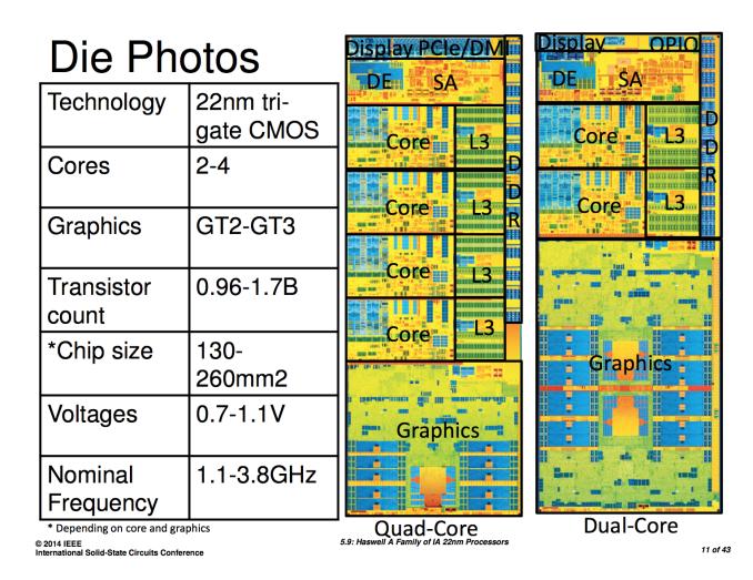
The first bit of new information we have are official transistor counts for the range of Haswell designs. At launch Intel only disclosed transistor counts and die areas for Haswell ULT GT3 (dual-core, on-die PCH, GT3 graphics) and Haswell GT2 (quad-core, no on-die PCH, GT2 graphics). Today we have both the minimum and maximum configurations for Haswell. Note all transistor counts below are schematic not layout:
| Intel Haswell | |||||||||||||||||
| CPU Configuration | GPU Configuration | Die Size | Transistor Count | ||||||||||||||
| 4+3 | Quad-Core | GT3e | 260mm2 + 77mm2 | 1.7B + ? | |||||||||||||
| ULT 2+3 | Dual-Core | GT3 | 181mm2 | 1.3B | |||||||||||||
| ULT 2+2 | Dual-Core | GT2 | ? | (est) ~1B | |||||||||||||
| 4+2 | Quad-Core | GT2 | 177mm2 | 1.4B | |||||||||||||
| 2+2 | Dual-Core | GT2 | 130mm2 | 0.96B | |||||||||||||
I've organized the table above by decreasing die size. I still don't have confirmation for the ULT 2+2 configuration, but the rest is now filled in and accurate. If you remember back to our Iris Pro review, I measured the die area for Haswell GT3 and the Crystalwell eDRAM using some cheap calipers. I came up with 264mm2 + 84mm2, the actual numbers are pretty close at 260mm2 + 77mm2.
Doing some rough math we see that the addition of a third graphics slice to a Haswell core accounts for around 300M transistors. That would put the ULT2+2 configuration at around 1B total transistors. I suspect the ULT 2+2 configuration is similar in size to the quad-core + GT2 configuration.
Next up on the list is some additional information on the Crystalwell (embedded DRAM) design and configuration. Intel explained how it arrived at the 128MB L4 eDRAM cache size, but it wouldn't tell us the operating frequency of the memory or the interface between it and the main CPU die. In its ISSCC disclosures, Intel filled in the blanks:
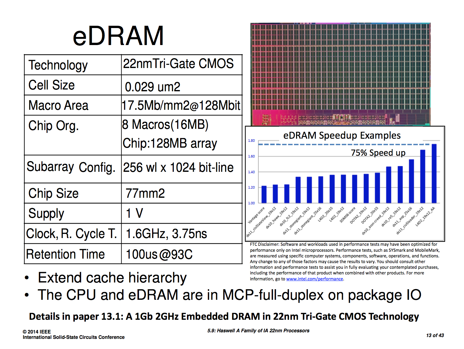
The 128MB eDRAM is divided among eight 16MB macros. The eDRAM operates at 1.6GHz and connects to the outside world via a 4 x 16-bit wide on-package IO (OPIO) interface capable of up to 6.4GT/s. The OPIO is highly scalable and very area/power efficient. The Haswell ULT variants use Intel's on-package IO to connect the CPU/GPU island to an on-package PCH. In this configuration the OPIO delivers 4GB/s of bandwidth at 1pJ/bit. When used as an interface to Crystalwell, the interface delivers up to 102GB/s at 1.22pJ/bit. That amounts to a little under 1.07W of power consumed to transmit/receive data at 102GB/s.
By keeping the eDRAM (or PCH) very close to the CPU island (1.5mm), Intel can make the OPIO extremely simple.
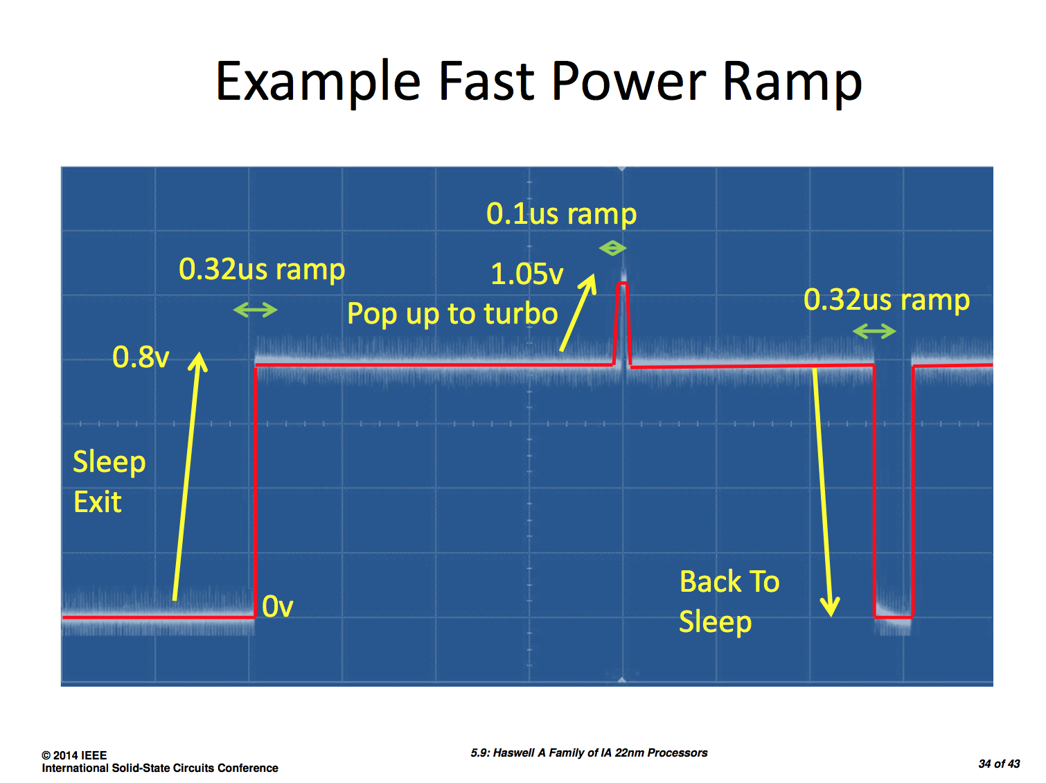
Intel also shared some data on how it achieved substantial power savings with Haswell, including using a new stacked power gate for the memory interface that reduced leakage by 100x over Ivy Bridge. Haswell's FIVR (Full Integrated Voltage Regulator) is also a topic of discussion in Intel's ISSCC papers. FIVR ends up being 90% efficient under load and can enter/exit sleep in 0.32µs, requiring only 0.1µs to ramp up to turbo frequencies.
Intel's Haswell ISSCC disclosures don't really change anything about Haswell, but they do further illustrate just how impressive of a design it is.


44 Comments
View All Comments
TiGr1982 - Monday, February 10, 2014 - link
No, Haswell refresh is expected to be just a minor clock speed bump with respect to current Haswell (and die stepping change at best), and, thus, compatible with the current LGA1150 socket for current Haswell line-up.As an argument supporting this state of things, Gigabyte recently (two weeks ago) released a new F8 BIOS for my M/B (Z87X-UD3H) stating "Support New 4th Generation Intel Core Processors", while all existing current Haswell models were already supported by previous BIOSes (F7 and earlier).
blanarahul - Sunday, February 9, 2014 - link
So. How many more years will it take to create the perfect architecture?? We are pretty close but how many years (months?) till we reach the limit??tipoo - Sunday, February 9, 2014 - link
Perfect is ill defined. Engineering is all about tradeoffs. One persons perfect processor is not anothers. That said, we've enjoyed gains in processor speeds in large part due to fabrication process shrinks and because of them more caches and transistors thrown at problems, and we should start hitting some weird issues after 14nm, so I'll be curious to see what the industry does after that, if they can keep shrinking, or if we'll be stuck there for a while with them only being able to focus on architecture to improve performance.YazX_ - Sunday, February 9, 2014 - link
@tipoo, couldnt agree more.purerice - Sunday, February 9, 2014 - link
Maybe by "perfect" s/he meant either the point where further (noticeable) efficiency is (virtually) impossible ( shrinks aside) or the point where things are "fast enough" for (virtually) any user. Or maybe the point where further efficiency gains can no longer (economically) be made.I'd really love to see AMD pull a rabbit out of a hat with their next CPU design. If they can't, I really hope ARM can. Haswell is an architectural masterpiece yet somehow at the desktop/workstation level fails to do much for performance/watt or OC over IB/SB. None of that makes much sense. If -Y and -U chips see major gains in graphics and general processing, why don't the -K chips too?
DanNeely - Sunday, February 9, 2014 - link
Because Intel's optimizing their CPU designs for increasingly low power levels. Instead of the sweet spot being between full power laptop CPUs and mid range desktops leaving a decent amount of head room above the top of the high end parts for additional OC the optimum is being centered on the low power laptop parts with the result that the equivalent of the OC gain from more power we used to get is being used up in the spread between full power laptop and desktop parts with very little left for those of us willing to crank the power up even higher.blanarahul - Monday, February 10, 2014 - link
That's precisely what I meant. Sorry, I wasn't clear enough in my first post.BMNify - Sunday, February 9, 2014 - link
"the perfect architecture" there's no such thing, even if you refer to something as simple as x264 encoding a UHD-1 video...for instance "Cisco is predicting a nearly 11-fold increase in global mobile data traffic over the next four years to reach 190 exabytes in 2018, with Asia Pacific leading the way ..."
the fact that by estimating the new haswell details numbers above its clear that you can't real time encode x264 UHD-1 3840×2160 video with high quality settings ,never mind do the real HEVC Main 10 profile UHD-2 7680×4320 digital broadcast expected in 3-6 years from now,
if you're asking what comes next to accommodate this massive data throughput for real time encoding for the masses then its probably going to be wideIO 2.5D then 3D High Bandwidth Memory , and then Si photonics in combination with these options....
although you just know that the antiquated server providers will try and keep that away from the masses as long as possible to keep their margins high
MrDiSante - Sunday, February 9, 2014 - link
The last two images in the article aren't showing up - if I try to open them directly I get a 404.dragonsqrrl - Sunday, February 9, 2014 - link
"I suspect the ULT 2+2 configuration is similar in size to the quad-core + GT2 configuration."Do you mean ULT 2+3?