NVIDIA Updates GPU Roadmap; Unveils Pascal Architecture For 2016
by Ryan Smith on March 26, 2014 2:30 AM EST
In something of a surprise move, NVIDIA took to the stage today at GTC to announce a new roadmap for their GPU families. With today’s announcement comes news of a significant restructuring of the roadmap that will see GPUs and features moved around, and a new GPU architecture, Pascal, introduced in the middle.
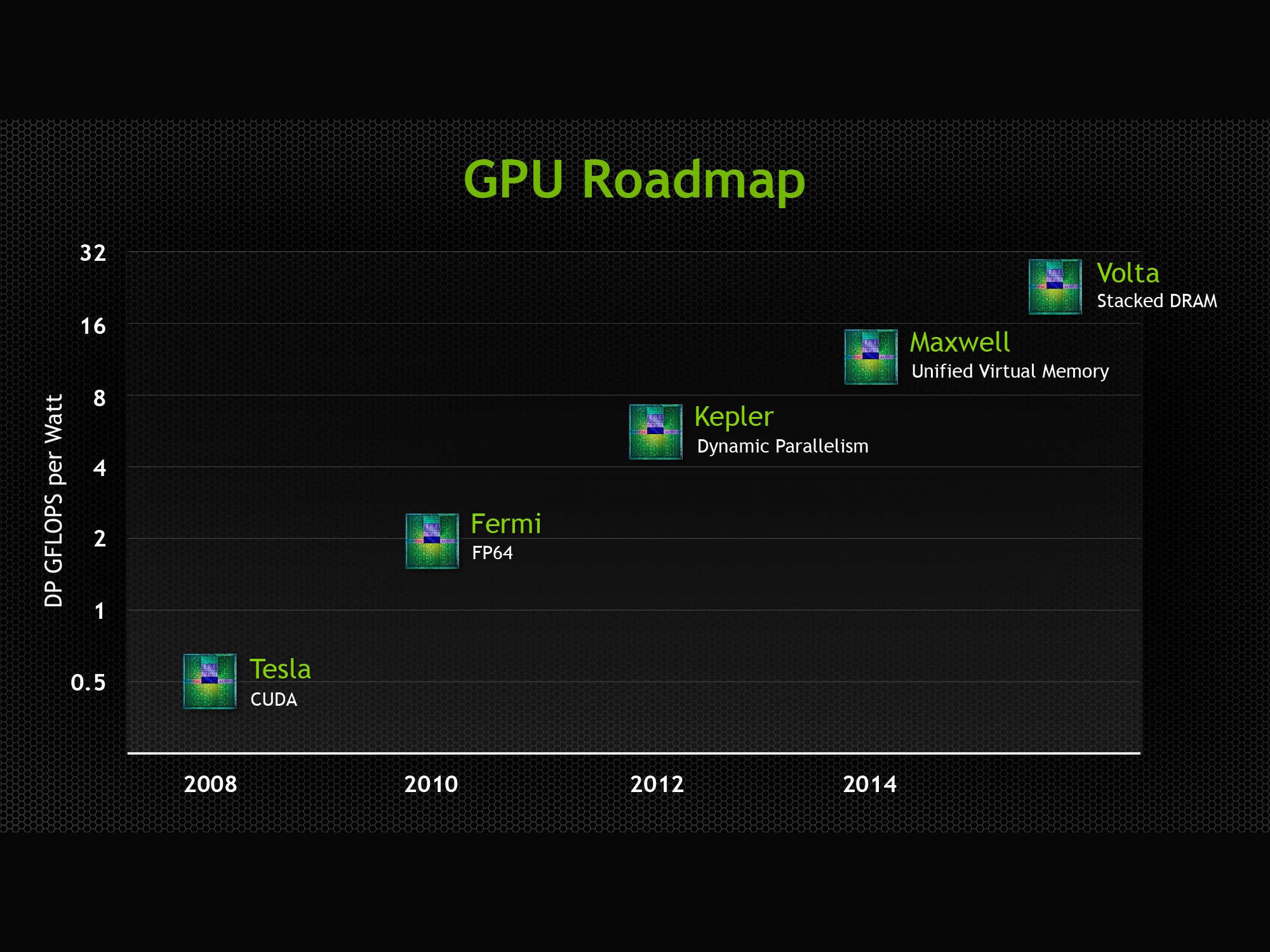
We’ll get to Pascal in a second, but to put it into context let’s first discuss NVIDIA’s restructuring. At GTC 2013 NVIDIA announced their future Volta architecture. Volta, which had no scheduled date at the time, would be the GPU after Maxwell. Volta’s marquee feature would be on-package DRAM, utilizing Through Silicon Vias (TSVs) to die stack memory and place it on the same package as the GPU. Meanwhile in that roadmap NVIDIA also gave Maxwell a date and a marquee feature: 2014, and Unified Virtual Memory.
NVIDIA's Old Volta Roadmap
NVIDIA's New Pascal Roadmap
As of today that roadmap has more or less been thrown out. No products have been removed, but what Maxwell is and what Volta is have changed, as has the pacing. Maxwell for its part has “lost” its unified virtual memory feature. This feature is now slated for the chip after Maxwell, and in the meantime the closest Maxwell will get is the software based unified memory feature being rolled out in CUDA 6. Furthermore NVIDIA has not offered any further details on second generation Maxwell (the higher performing Maxwell chips) and how those might be integrated into professional products.
As far as NVIDIA is concerned, Maxwell’s marquee feature is now DirectX 12 support (though even the extent of this isn’t perfectly clear), and that with the shipment of the GeForce GTX 750 series, Maxwell is now shipping in 2014 as scheduled. We’re still expecting second generation Maxwell products, but at this juncture it does not look like we should be expecting any additional functionality beyond what Big Kepler + 1st Gen Maxwell can achieve.
Meanwhile Volta has been pushed back and stripped of its marquee feature. It’s on-package DRAM has been promoted to the GPU before Volta, and while Volta still exists, publicly it is a blank slate. We do not know anything else about Volta beyond the fact that it will come after the 2016 GPU.
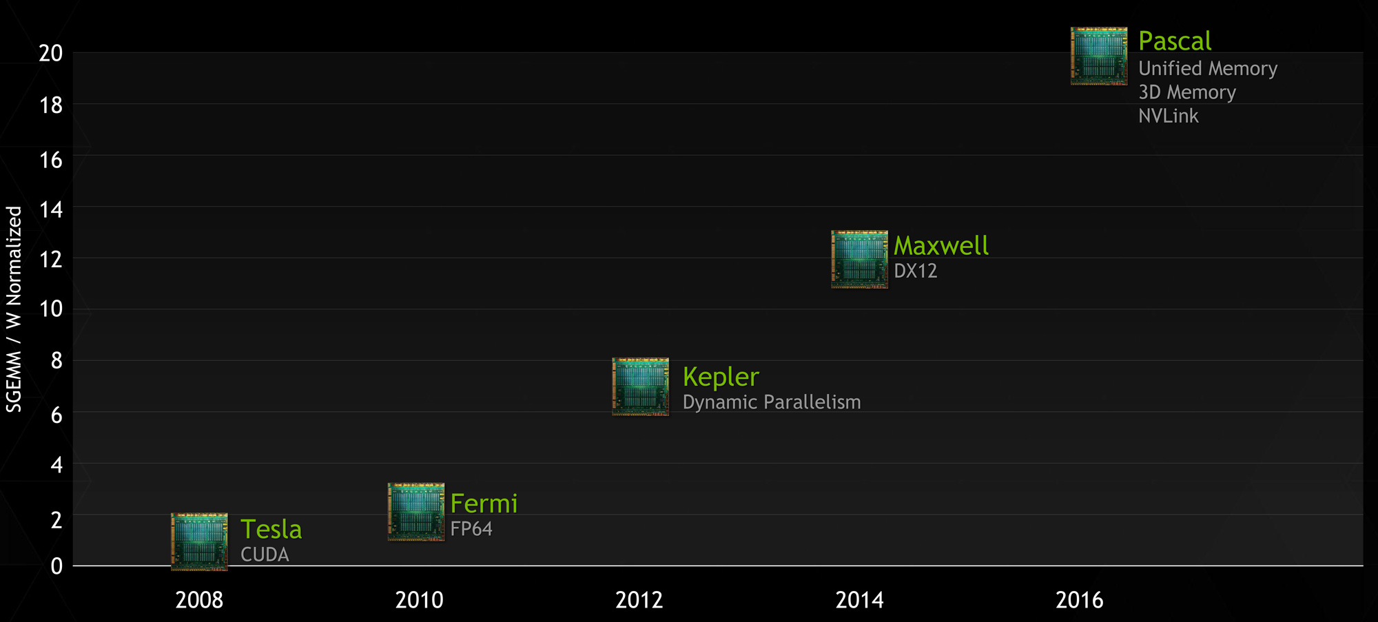
Which brings us to Pascal, the 2016 GPU. Pascal is NVIDIA’s latest GPU architecture and is being introduced in between Maxwell and Volta. In the process it has absorbed old Maxwell’s unified virtual memory support and old Volta’s on-package DRAM, integrating those feature additions into a single new product.
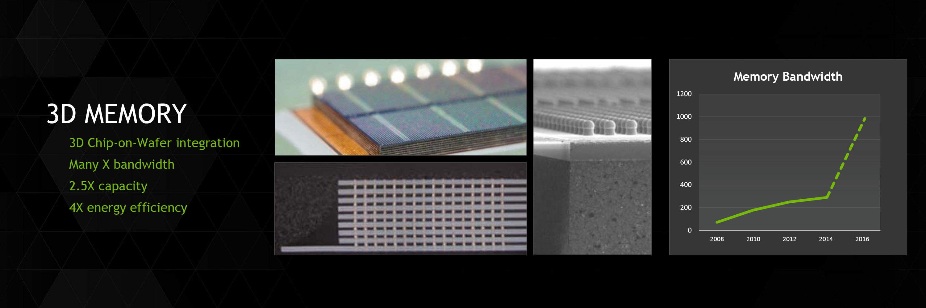
With today’s announcement comes a small degree of additional detail on NVIDIA’s on-package memory plans. The bulk of what we wrote for Volta last year remains true: NVIDIA uses on-package stacked DRAM, allowed by the use of TSVs. What’s new is that NVIDIA has confirmed they will be using JEDEC’s High Bandwidth Memory (HBM) standard, and the test vehicle Pascal card we have seen uses entirely on-package memory, so there isn’t a split memory design. Though we’d also point out that unlike the old Volta announcement, NVIDIA isn’t listing any solid bandwidth goals like the 1TB/sec number we had last time. From what NVIDIA has said, this likely comes down to a cost issue: how much memory bandwidth are customers willing to pay for, given the cutting edge nature of this technology?
Meanwhile NVIDIA hasn’t said anything else directly about the unified memory plans that Pascal has inherited from old Maxwell. However after we get to the final pillar of Pascal, how that will fit in should make more sense.
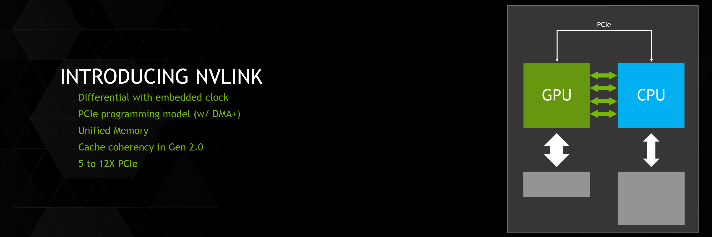
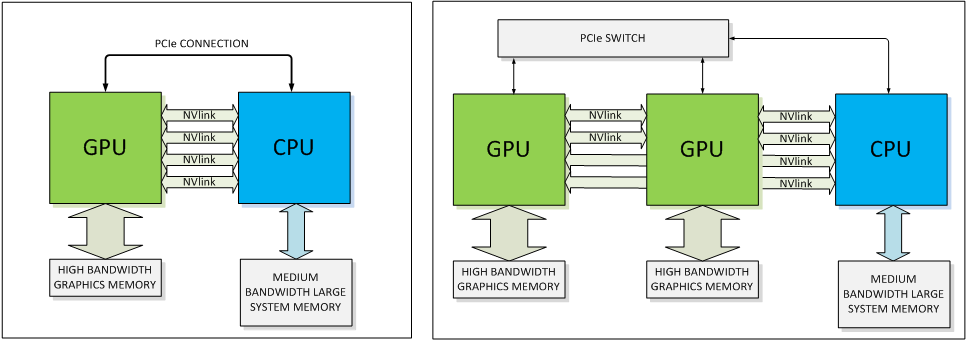
Coming to the final pillar then, we have a brand new feature being introduced for Pascal: NVLink. NVLink, in a nutshell, is NVIDIA’s effort to supplant PCI-Express with a faster interconnect bus. From the perspective of NVIDIA, who is looking at what it would take to allow compute workloads to better scale across multiple GPUs, the 16GB/sec made available by PCI-Express 3.0 is hardly adequate. Especially when compared to the 250GB/sec+ of memory bandwidth available within a single card. PCIe 4.0 in turn will eventually bring higher bandwidth yet, but this still is not enough. As such NVIDIA is pursuing their own bus to achieve the kind of bandwidth they desire.
The end result is a bus that looks a whole heck of a lot like PCIe, and is even programmed like PCIe, but operates with tighter requirements and a true point-to-point design. NVLink uses differential signaling (like PCIe), with the smallest unit of connectivity being a “block.” A block contains 8 lanes, each rated for 20Gbps, for a combined bandwidth of 20GB/sec. In terms of transfers per second this puts NVLink at roughly 20 gigatransfers/second, as compared to an already staggering 8GT/sec for PCIe 3.0, indicating at just how high a frequency this bus is planned to run at.
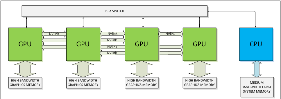
Multiple blocks in turn can be teamed together to provide additional bandwidth between two devices, or those blocks can be used to connect to additional devices, with the number of bricks depending on the SKU. The actual bus is purely point-to-point – no root complex has been discussed – so we’d be looking at processors directly wired to each other instead of going through a discrete PCIe switch or the root complex built into a CPU. This makes NVLink very similar to AMD’s Hypertransport, or Intel’s Quick Path Interconnect (QPI). This includes the NUMA aspects of not necessarily having every processor connected to every other processor.
But the rabbit hole goes deeper. To pull off the kind of transfer rates NVIDIA wants to accomplish, the traditional PCI/PCIe style edge connector is no good; if nothing else the lengths that can be supported by such a fast bus are too short. So NVLink will be ditching the slot in favor of what NVIDIA is labeling a mezzanine connector, the type of connector typically used to sandwich multiple PCBs together (think GTX 295). We haven’t seen the connector yet, but it goes without saying that this requires a major change in motherboard designs for the boards that will support NVLink. The upside of this however is that with this change and the use of a true point-to-point bus, what NVIDIA is proposing is for all practical purposes a socketed GPU, just with the memory and power delivery circuitry on the GPU instead of on the motherboard.
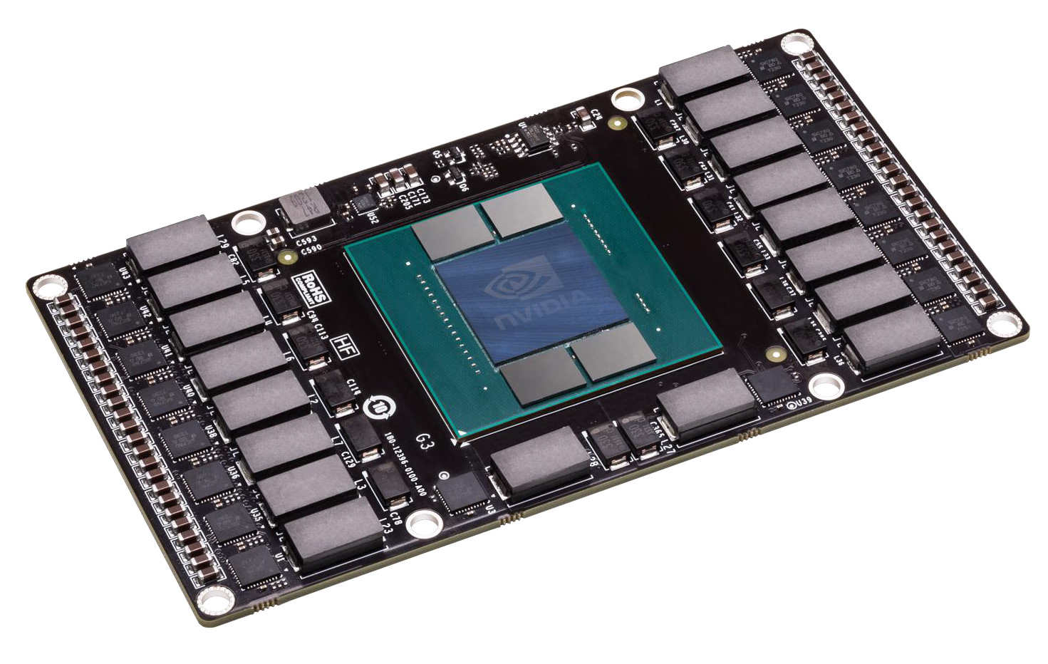
NVIDIA’s Pascal test vehicle is one such example of what a card would look like. We cannot see the connector itself, but the basic idea is that it will lay down on a motherboard parallel to the board (instead of perpendicular like PCIe slots), with each Pascal card connected to the board through the NVLink mezzanine connector. Besides reducing trace lengths, this has the added benefit of allowing such GPUs to be cooled with CPU-style cooling methods (we’re talking about servers here, not desktops) in a space efficient manner. How many NVLink mezzanine connectors available would of course depend on how many the motherboard design calls for, which in turn will depend on how much space is available.
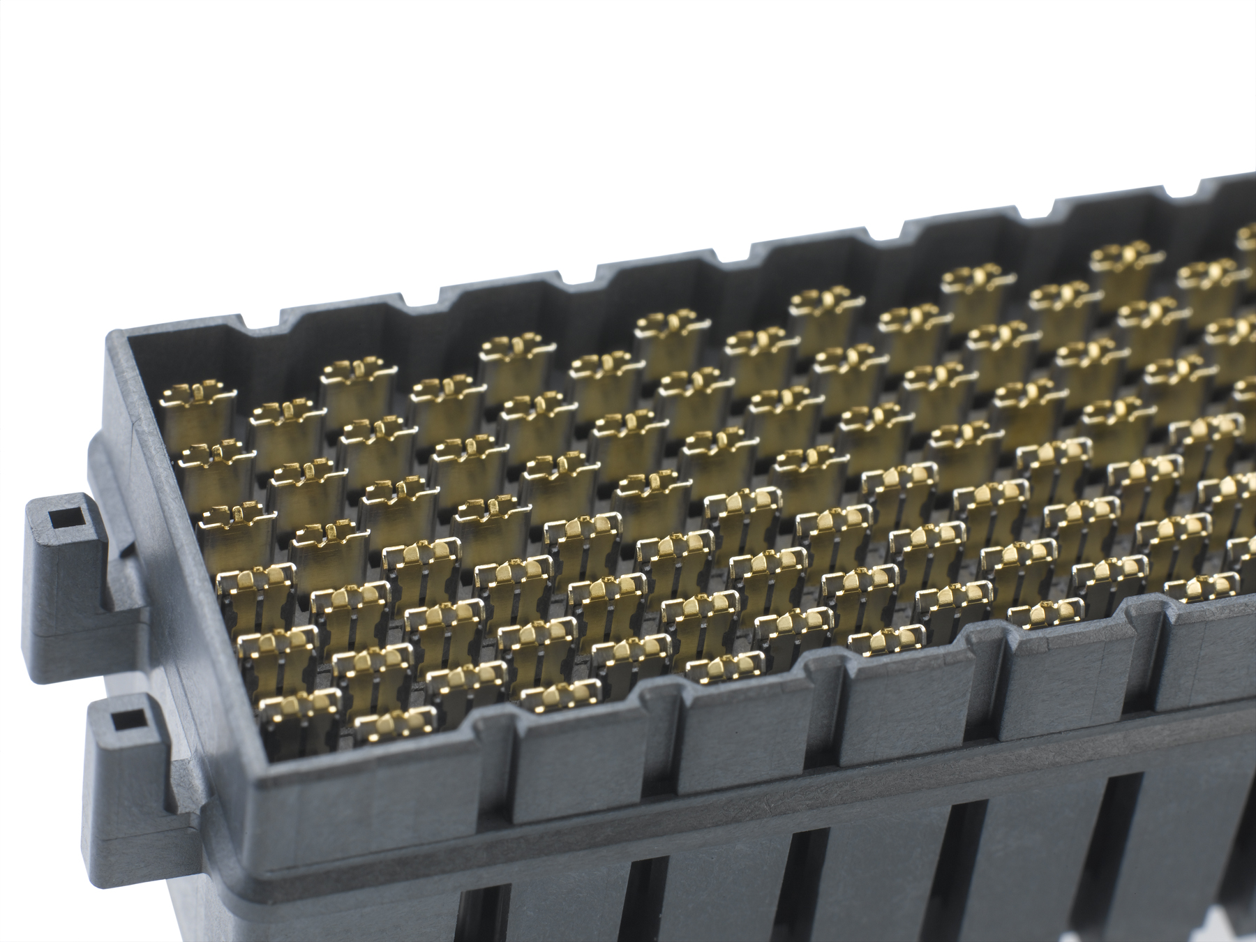
Molex's NeoScale: An example of a modern, high bandwidth mezzanine connector
One final benefit NVIDIA is touting is that the new connector and bus will improve both energy efficiency and energy delivery. When it comes to energy efficiency NVIDIA is telling us that per byte, NVLink will be more efficient than PCIe – this being a legitimate concern when scaling up to many GPUs. At the same time the connector will be designed to provide far more than the 75W PCIe is spec’d for today, allowing the GPU to be directly powered via the connector, as opposed to requiring external PCIe power cables that clutter up designs.
With all of that said, while NVIDIA has grand plans for NVLink, it’s also clear that PCIe isn’t going to be completely replaced anytime soon on a large scale. NVIDIA will still support PCIe – in fact the blocks can talk PCIe or NVLink – and even in NVLink setups there are certain command and control communiques that must be sent through PCIe rather than NVLink. In other words, PCIe will still be supported across NVIDIA's product lines, with NVLink existing as a high performance alternative for the appropriate product lines. The best case scenario for NVLink right now is that it takes hold in servers, while workstations and consumers would continue to use PCIe as they do today.
Meanwhile, though NVLink won’t even be shipping until Pascal in 2016, NVIDIA already has some future plans in store for the technology. Along with a GPU-to-GPU link, NVIDIA’s plans include a more ambitious CPU-to-GPU link, in large part to achieve the same data transfer and synchronization goals as with inter-GPU communication. As part of the OpenPOWER consortium, NVLink is being made available to POWER CPU designs, though no specific CPU has been announced. Meanwhile the door is also left open for NVIDIA to build an ARM CPU implementing NVLink (Denver perhaps?) but again, no such product is being announced today. If it did come to fruition though, then it would be similar in concept to AMD’s abandoned “Torrenza” plans to utilize HyperTransport to connect CPUs with other processors (e.g. GPUs).
Finally, NVIDIA has already worked out some feature goals for what they want to do with NVLink 2.0, which would come on the GPU after Pascal (which by NV’s other statements should be Volta). NVLink 2.0 would introduce cache coherency to the interface and processors on it, which would allow for further performance improvements and the ability to more readily execute programs in a heterogeneous manner, as cache coherency is a precursor to tightly shared memory.
Wrapping things up, with an attached date for Pascal and numerous features now billed for that product, NVIDIA looks to have to set the wheels in motion for developing the GPU they’d like to have in 2016. The roadmap alteration we’ve seen today is unexpected to say the least, but Pascal is on much more solid footing than old Volta was in 2013. In the meantime we’re still waiting to see what Maxwell will bring NVIDIA’s professional products, and it looks like we’ll be waiting a bit longer to get the answer to that question.


68 Comments
View All Comments
JBVertexx - Wednesday, March 26, 2014 - link
Lack of competition, they're essentially able to take the foot off the development gas pedal.Mr Perfect - Wednesday, March 26, 2014 - link
Well, that and a lack of a node shrink. We've been stuck on 28nm for what? Almost three years now?extide - Wednesday, March 26, 2014 - link
Uhhh... not really... we aren't talking about Intel vs AMD here, The R9 290x is very competitive.jasonelmore - Thursday, March 27, 2014 - link
Performance per watt man. mobile outsells desktops 10:1Lonyo - Wednesday, March 26, 2014 - link
Did NV just talk generally about NVLink or was there an HPC context to the discussions?Presumably if they are still supporting PCIe they are going for totally different cards for HPC/etc use vs standard personal computers? Maybe with an eventual long term desktop transition to NVLink if it ever makes sense.
Ryan Smith - Wednesday, March 26, 2014 - link
The context for NVLink is almost entirely HPC. There is the potential to use it elsewhere, but at the start its best chances are in custom HPC hardware.Yojimbo - Wednesday, March 26, 2014 - link
Doesn't it seem difficult to imagine NVLink to be used in maintstream PC/notebook gaming systems without Intel being on board? It seems either multi-GPU setups would become mainstream, NVidia would have a secondary CPU across the PCI-E bus from the primary CPU, or NVidia would attempt to replace the x86 CPU entirely, somehow, in order for NVLink to be used for GPU-GPU or GPU-CPU communication in mainstream PC/notebook gaming systems without Intel being part of it. Or am I thinking about something incorrectly?In any case, Intel might look at it as a threat. They probably want to control all infrastructure themselves. They can't stop IBM and NVidia from hammering out an effective computing platform in the HPC space that may eventually beg to be brought to more mainstream computing. Maybe, if the system is effective, they might have to copy it with Phi (or perhaps they are already developing something in parallel), assuming Phi is competitive with GPUs.
When AMD made HyperTransport, Intel didn't use it, they developed QPI, isn't it?
BMNify - Thursday, March 27, 2014 - link
you are right unless they have a way to bypass the limited QPI and HyperTransport interconnects to get more data throughput , remember that's at Intel and AMD's whimQPI "Intel describes the data throughput (in GB/s) by counting only the 64-bit data payload in each 80-bit "flit". However, Intel then doubles the result because the unidirectional send and receive link pair can be simultaneously active. Thus, Intel describes a 20-lane QPI link pair (send and receive) with a 3.2 GHz clock as having a data rate of 25.6 GB/s. A clock rate of 2.4 GHz yields a data rate of 19.2 GB/s. More generally, by this definition a two-link 20-lane QPI transfers eight bytes per clock cycle, four in each direction.
The rate is computed as follows:
3.2 GHz
× 2 bits/Hz (double data rate)
× 16(20) (data bits/QPI link width)
× 2 (unidirectional send and receive operating simultaneously)
÷ 8 (bits/byte)
= 25.6 GB/s"
"HyperTransport supports an autonegotiated bit width, ranging from 2 to 32 bits per link; there are two unidirectional links per HyperTransport bus. With the advent of version 3.1, using full 32-bit links and utilizing the full HyperTransport 3.1 specification's operating frequency, the theoretical transfer rate is 25.6 GB/s (3.2 GHz × 2 transfers per clock cycle × 32 bits per link) per direction, or 51.2 GB/s aggregated throughput, making it faster than most existing bus standard for PC workstations and servers as well as making it faster than most bus standards for high-performance computing and networking.
Links of various widths can be mixed together in a single system configuration as in one 16-bit link to another CPU and one 8-bit link to a peripheral device, which allows for a wider interconnect between CPUs, and a lower bandwidth interconnect to peripherals as appropriate. It also supports link splitting, where a single 16-bit link can be divided into two 8-bit links. The technology also typically has lower latency than other solutions due to its lower overhead."
from the open PPC IBM initiative they can make and use any new NOC (network On Chip) they like or take another's generic NOC IP to get near their real 250GB/sec over 8 links NVLink block, ARM have generic IP for a 256GB/sec NOC (2Tb/s) for instance, as does MoSys
"MoSys today announced the architecture for its third generation Bandwidth Engine® family, featuring the industry's highest serial throughput and memory access rate, optimized efficiency and scheduling for multi-core processing, and expanded multi-cycle embedded macro functions. MoSys today announced the architecture for its third generation Bandwidth Engine® family, featuring the industry's highest serial throughput and memory access rate, optimized efficiency and scheduling for multi-core processing, and expanded multi-cycle embedded macro functions. MoSys today announced the architecture for its third generation Bandwidth Engine® family, featuring the industry's highest serial throughput and memory access rate, optimized efficiency and scheduling for multi-core processing, and expanded multi-cycle embedded macro functions. MoSys today announced the architecture for its third generation Bandwidth Engine® family, featuring the industry's highest serial throughput and memory access rate, optimized efficiency and scheduling for multi-core processing, and expanded multi-cycle embedded macro functions, as does MoSys today announced the architecture for its third generation Bandwidth Engine® family, featuring the industry's highest serial throughput and memory access rate, optimized efficiency and scheduling for multi-core processing, and expanded multi-cycle embedded macro functions. "
OC non of this matter's unless they have a way to interface the x86 directly over a new internal NOC on the CPU's die bypassing the QuickPath Interconnect,the even slower DMI 2.0, the HyperTransport, and the PCI-E bus.... theres a reason they are working with a CPU vendor that can add the needed modern NOC they required to push these data rates to the cores...
unless Ryan, annand or anyone else can say how they will add this new NVLink to intel chips and keep that up to 256GB/sec potential !
BMNify - Thursday, March 27, 2014 - link
oops, sorry for the bad C&P, by the way Ryan, any idea Why they went for HBM and not the better lower power and more configurable HMC on HMC on substrate so early on.dj_aris - Wednesday, March 26, 2014 - link
Nvidia are a bit over-confident I think. NVlink is great and all but who is going to support them? I think that such a drastic change in motherboard design isn't going to be allowed by chipset providers (Intel wouldn't even allow them to build chipset beyond Core 2 Duo and AMD, well why would they change their chipsets design for a competitor's plan?) PCs indeed need to shrink (all-in-one motherboards are obviously the right direction) but not that soon. Maybe Intel and AMD should create the new PCIe connector, maybe MXM-type.