Samsung SSD 845DC EVO/PRO Performance Preview & Exploring IOPS Consistency
by Kristian Vättö on September 3, 2014 8:00 AM ESTSamsung SSD 845DC PRO
| Samsung SSD 845DC PRO | |||||
| Capacity | 400GB | 800GB | |||
| Controller | Samsung MDX | ||||
| NAND | Samsung 128Gbit 24-layer 40nm MLC V-NAND | ||||
| Sequential Read | 530MB/s | 530MB/s | |||
| Sequential Write | 460MB/s | 460MB/s | |||
| 4KB Random Read | 92K IOPS | 92K IOPS | |||
| 4KB Random Write | 50K IOPS | 51K IOPS | |||
| Idle Power | 1.0W | 1.0W | |||
| Load Power (Read/Write) | 1.7W / 3.1W | 1.7W / 3.3W | |||
| Endurance (TBW) | 7,300TB | 14,600TB | |||
| Endurance (DWPD) | 10 DWPD | ||||
| Warranty | Five years | ||||
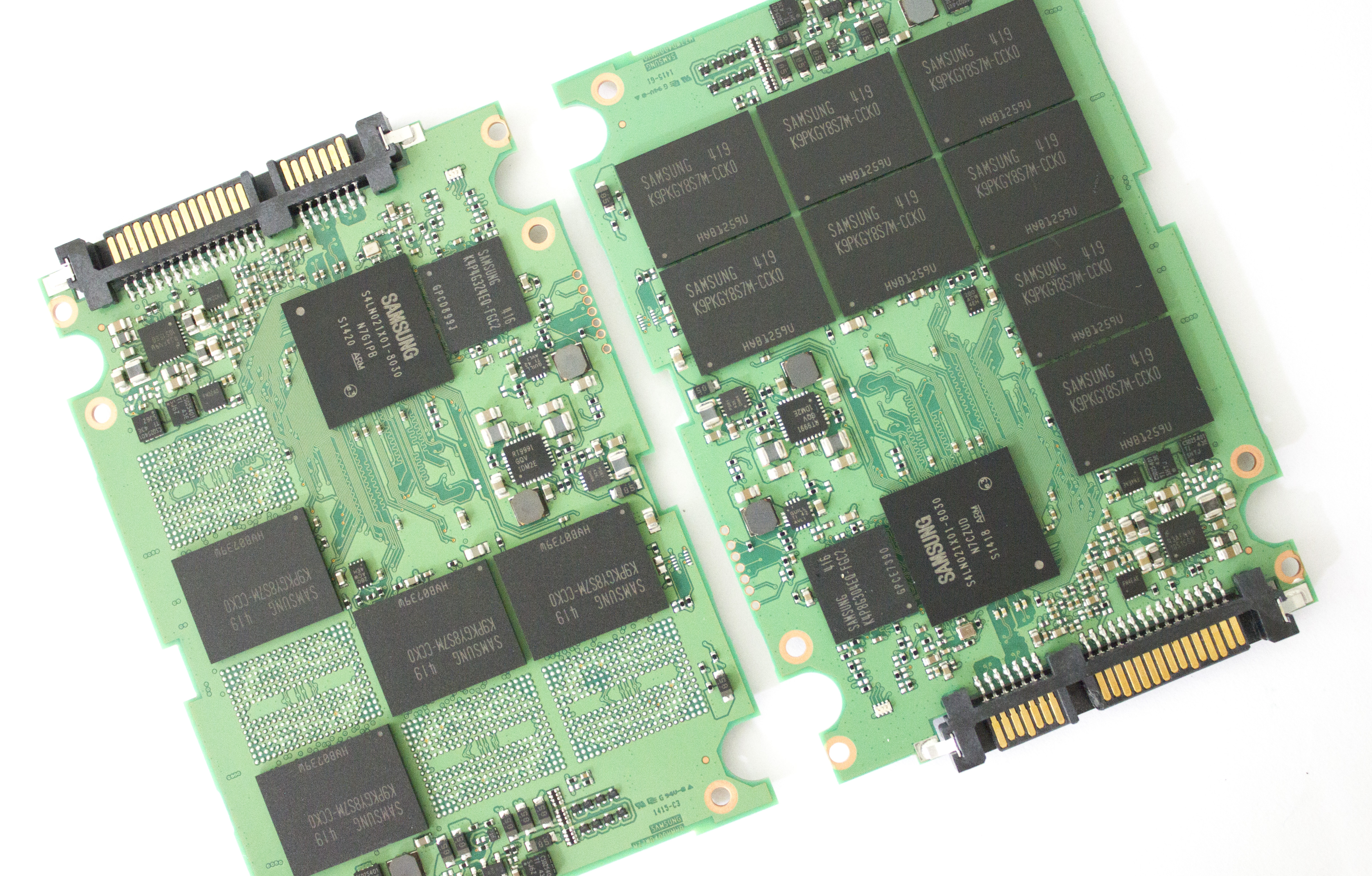
Surprisingly the 845DC PRO goes for the older MDX controller that was used in the SSD 840 and 840 Pro. Architecturally the MDX and MEX are the same since both are based on the 3-core ARM Cortex R4 base, but the MEX just runs at a higher clock speed (400MHz vs 300MHz). I suspect the MEX controller does not really offer a major benefit for MLC NAND based SSDs because there is much less NAND management to do, but with TLC the extra processing power is certainly useful given the amount of ECC and management TLC needs.
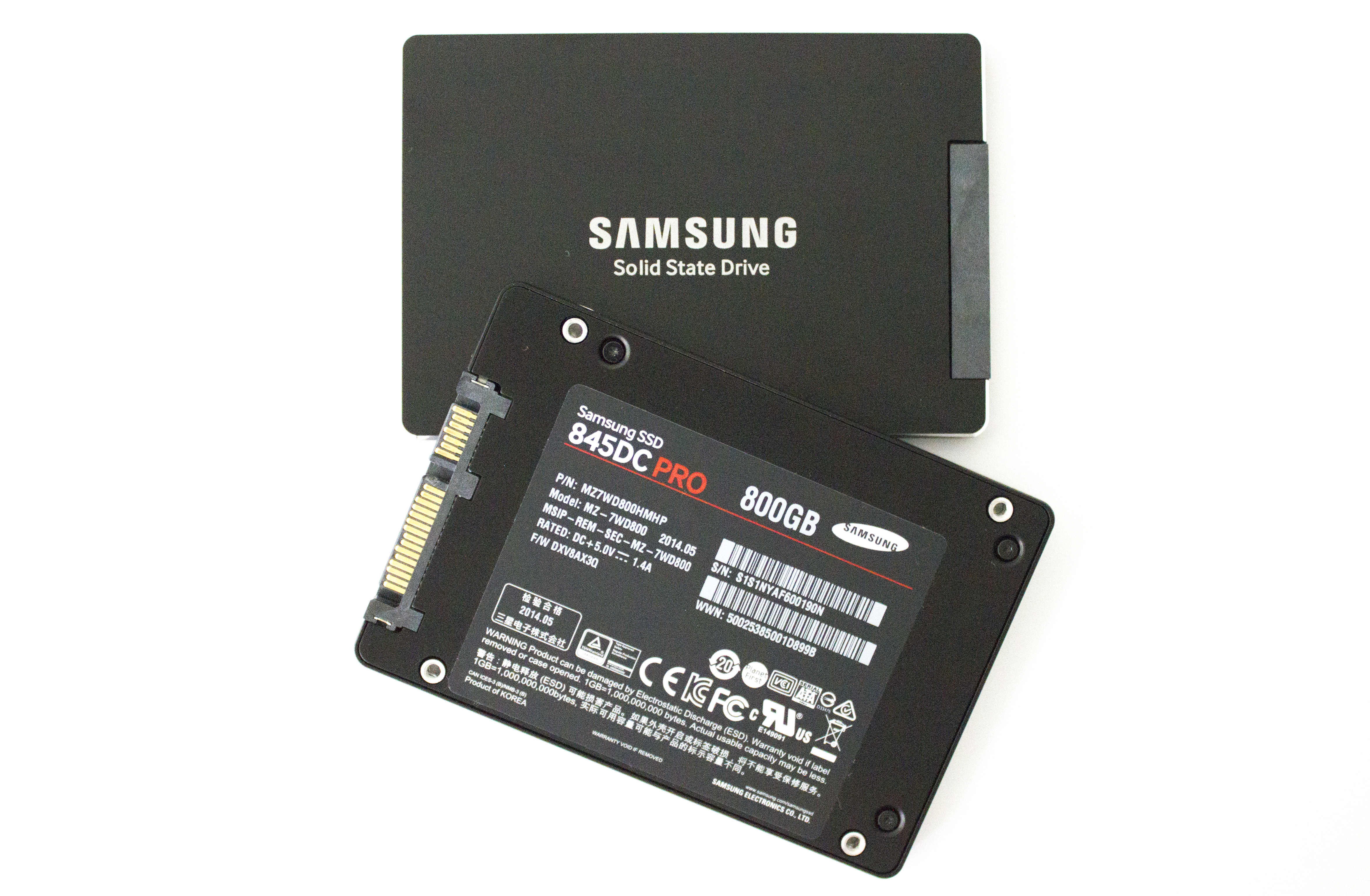
The 845DC PRO is only available in two capacities: 400GB and 800GB. I heard Samsung has plans to add a higher capacity version (1,600GB?) later on but for the time being the 845DC PRO is limited to just 800GB. I suspect that going above 1TiB of raw NAND requires a controller update, which would explain why higher capacities are not available yet. In the end, the 845DC PRO is using silicon that is now two years old, which adds some design limitations.
Similar to the 845DC EVO, the PRO has capacitors that offer data protection in case of a power loss.
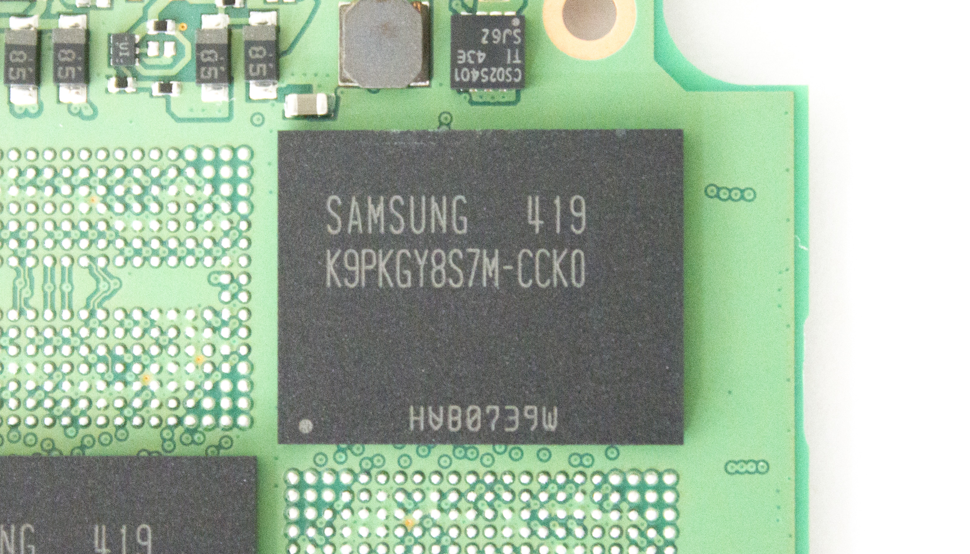
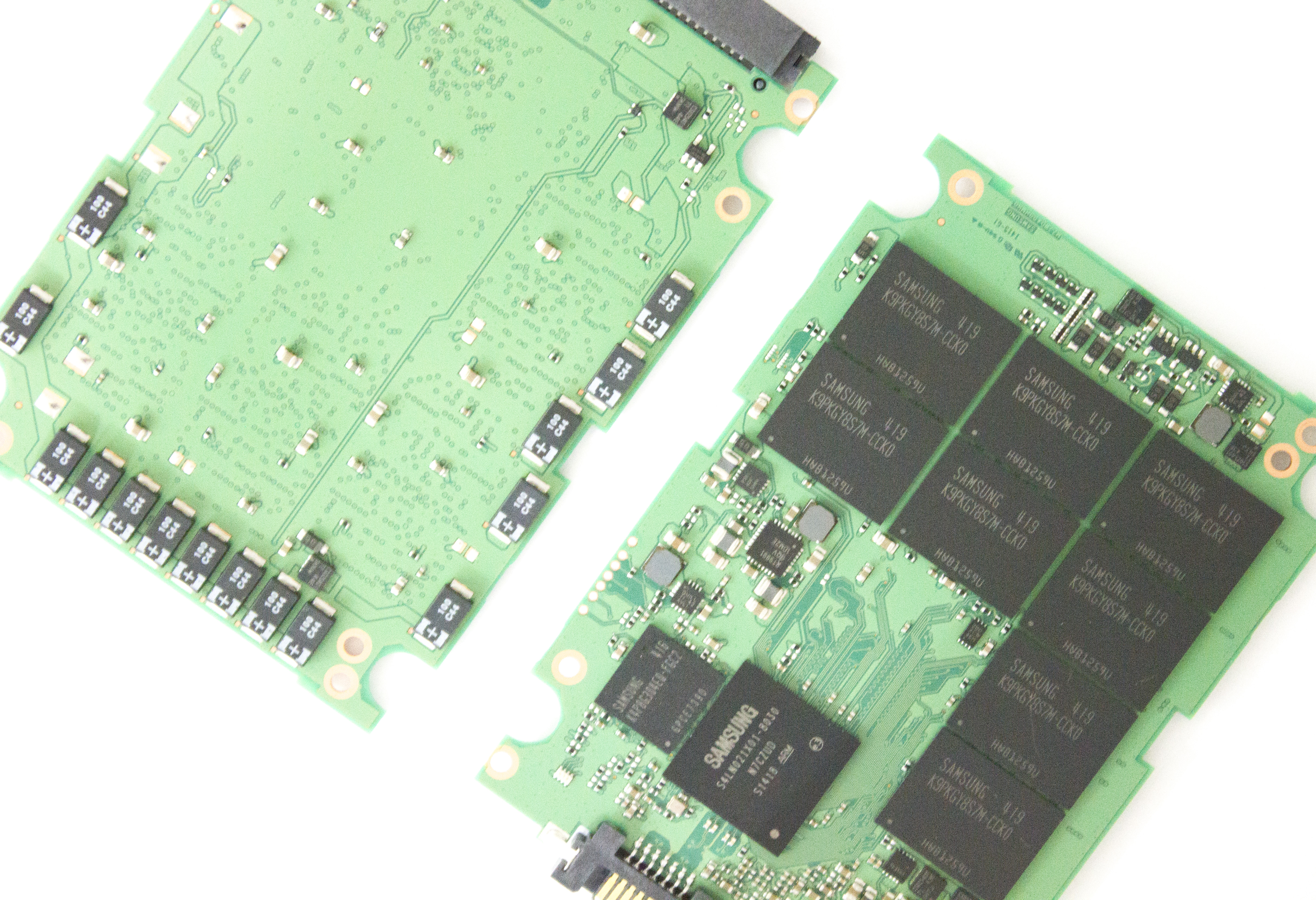
The 845DC PRO uses Samsung's first generation V-NAND, which is a 24-layer design with a die capacity of 128Gbit. The part numbers of the first and second generation are almost equal and the only way to distinquish the two is to look at the third, fourth and fifth characters since they reveal the number of die per package as well as the total capacity of the package. Our 400GB sample has four and our 800GB has eight 8-die packages on the PCB, so the raw NAND capacities work out to be 512GiB and 1024GiB respectively with over-provisioning being 28%.
I am not going to cover V-NAND in detail here as I did that in the 850 Pro review and architecturally the first generation V-NAND is no different – it is just 24 layers instead of 32. The first generation is an older, more mature process and thus more suitable for enterprise SSDs. I measured the endurance of the first generation V-NAND to be 40,000 P/E cycles, whereas the second generation V-NAND in the 850 Pro is only rated at 6,000 P/E cycles. For the record, you would either need eMLC or SLC to get 40,000 P/E cycles with 2D NAND, but V-NAND does that while being normal MLC. The benefit over eMLC is performance as eMLC sacrifices program and erase latencies for higher endurance, and the eMLC manufacturing process is also more complicated than regular MLC (although I am pretty sure that V-NAND is still more complicated and hence more expensive).


31 Comments
View All Comments
Inds - Wednesday, February 4, 2015 - link
Ok, this doesn't clear anything up. If my manufacturer is lying about the IOPS of my SSD, how do I figure out the real value?If they aren't lying about the 97,000 random read IOPS, how many megabytes per second is this for 4KB?
What exactly is the formula? You never elaborate on this in the article beyond senseless ramble.
First of all, how am I gonna know what the queue length even is? The way I see it on benchmark tests, low queue depths have lower MB/s than higher ones so this confuses the hell out of me.
But okay, I wanna know how my 840 Evo will perform random reads in the worst case scenario and QD1 seems to be the worst case scenario according to all the benchmark evidence.
In that case, I must time the QD by the latency. My latency I believe is 1 ms so my result is 1000. 1000 IOPS? Okay, so my 4KB random read speed will be 4 MB/s? That's nowhere close to the real result CrystalDiskMark shows.