Samsung Announces 14nm FinFET for Exynos 7
by Joshua Ho on February 16, 2015 4:04 AM EST- Posted in
- Smartphones
- Mobile
- Tablets
- SoCs
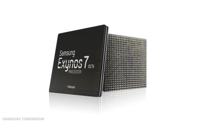
While we've known about the existence of the Exynos 7420 for a while now, we didn't really know what to expect until recently. Today, it seems that Samsung is ready to start disclosing at least a few details about an upcoming Exynos 7 SoC, which is likely to be the Exynos 7420.
At a high level Exynos 7 will have four Cortex A57s clocked at 2.1 GHz, in addition to four Cortex A53s along with an LPDDR4-capable memory interface. According to Samsung Tomorrow, we can expect a 20% increase to device performance, which is likely a reference to clock speed, and 35% lower power consumption. In addition, there is a reference to a 30% productivity gain, which is likely to be referencing performance per watt. Samsung claims that these figures come from a comparison to their 20nm HKMG process, which we've examined before with the Exynos 5433 in the Note 4 Exynos review.
Although there is no direct statement of which version of 14nm is used for this upcoming Exynos 7 Octa, judging by how this is the first 14nm IC to come from Samsung it's likely that this SoC will use 14LPE, which focuses on reducing leakage and power consumption rather than switching speed.
Source: Samsung Tomorrow


111 Comments
View All Comments
patrickjp93 - Tuesday, February 17, 2015 - link
But Samsung has only published claims about yields for its own processors. No one has 20nm chips out yet made by them, and Qualcomm and Apple only just jumped to Samsung a couple months ago, Nvidia much more recently. We have no proof of yields yet.JoshHo - Monday, February 16, 2015 - link
It's important to note that this process uses 20nm BEOL so it isn't quite comparable to Intel's 14nm process.krumme - Monday, February 16, 2015 - link
Density is probably more or less the same, due to interconnect, as evident from other comparisons. If this goes to S6 - and it looks like - yield is not an issue either.This process is tuned for mobile devices and not high perf as Intel - thats the difference - so its comparing apples to oranges. But for low power mobile devices Samsung now have a proces lead to Intel - and it looks like the arch is nice and small.
As a sidenote the LPDDR4 will make sure the GPU is fast as well as evident from prior 20nm 810 AT review.
What is questionable is DSP perf. , modem perf/watt, everything outside the GPU/CPU - that
Yojimbo - Monday, February 16, 2015 - link
Density does not seem to be the same:https://www.semiwiki.com/forum/content/3884-who-wi...
Krysto - Monday, February 16, 2015 - link
Only the interconnects are 20nm and the transistors are 14nm. I think Intel did something similar with its "22nm Trigate" process for Ivy Bridge and Haswell. I think they had 22nm interconnects with 26nm transistors. So Intel's "22nm" wasn't a pure 22nm either.Yojimbo - Monday, February 16, 2015 - link
Yes, Intel's 22nm node was less dense than Samsung's and TSMC's. But what does that have to do with the 14nm node?patrickjp93 - Tuesday, February 17, 2015 - link
And to be fair, Samsung and TSMC arrived at "28 nm" much later, and with AMD's HDL research, they pushed 28nm farther down than its original design plans. Now with FinFET added the rest of the industry seems to have taken a backstep in density the way Intel did, but it saves them dealing with massive leakage currents that the planar process was making far too problematic.III-V - Monday, February 16, 2015 - link
Node names have nothing to do with the process dimensions. It's been like this for decades:http://spectrum.ieee.org/semiconductors/devices/th...
witeken - Monday, February 16, 2015 - link
There's no such thing as a "14", "16", "22", "26", etc. *transistor*. The easiest way to (roughly) compare transistors is to look at their features: does it have HKMG, FinFET, etc. and at which generation?Right now, Intel is in its 2nd gen FinFET (14nm) while Samsung and TSMC only have 2nd gen HKMGs (20nm). This puts Intel roughly 2 nodes ahead in terms of transistor characteristics.
The easiest way to compare density/interconnect is to multiply 2 feature sizes (which can be obtained by measuring them like Chipworks does or using publicized data), after which you can get such a graph for density: http://image.ofweek.com/uploadfile/newsimg/b/2014/... This is only a rough comparison too because a process node always has multiple flavors like high density for SoCs and high performance for CPUs etc.
phoenix_rizzen - Monday, February 16, 2015 - link
When clicking that image link:403 Forbidden
nginx