The Intel Broadwell Desktop Review: Core i7-5775C and Core i5-5675C Tested (Part 1)
by Ian Cutress on June 2, 2015 7:45 AM EST
On almost all PC technology forums, it is hard to escape users talking about what Intel’s next processor lineup will be. Due to initial yield issues in Intel’s 14nm node, Broadwell in both mobile and desktop ended up being delayed, somewhat substantially in the case of the desktop. So while motherboard manufacturers released their Z97 platform over 6 months ago, we have been waiting for Broadwell to arrive. That day is today, and we can lay the smackdown with some benchmark numbers too.
The Road to Broadwell
Broadwell, in its top level explanation, is the 14nm die shrink of Haswell which was built on 22nm. Using Intel’s 14nm process this results in a smaller silicon die and lower power consumption. Frequency will depend on the architecture and if the process is suited to frequency or power, but the CPU core underneath is still more-or-less Haswell, with some minor tweaks of course.
As part of Intel’s tick-tock strategy, this would be considered a tick:
| Intel's Tick-Tock Cadence | |||||
| Microarchitecture | Process Node | Tick or Tock | Release Year | ||
| Conroe/Merom | 65nm | Tock | 2006 | ||
| Penryn | 45nm | Tick | 2007 | ||
| Nehalem | 45nm | Tock | 2008 | ||
| Westmere | 32nm | Tick | 2010 | ||
| Sandy Bridge | 32nm | Tock | 2011 | ||
| Ivy Bridge | 22nm | Tick | 2012 | ||
| Haswell | 22nm | Tock | 2013 | ||
| Broadwell | 14nm | Tick | Core-M: 2014 Others: 2015 |
||
If history tells us anything, ticks are usually accompanied by small IPC increases, resulting in 5-10% better performance depending on the benchmark, but ultimately ticks still follow the same capabilities of the processor before them. Intel usually uses its ticks to introduce a new chipset with a large number of capabilities, which we saw with Z97 and its use of M.2/SATA Express on the chipset. If the classical idea of a three year cycle between upgrades is true, then back in the summer of 2012, we were playing around with Ivy Bridge, the tick to Sandy Bridge.
The Broadwell Launch
Back in mid 2014, Intel launched Core M, the first 14nm processor in the mass market and the first Broadwell based product. Core M is the official marketing designation for what was historically the Y series processor (Broadwell-Y), but Core M played a different role to other Y series processors. Core M brought the Core architecture down to a 4.5W thermal design, enabling small and thin fanless 2-in-1 laptop/tablet designs. When the first products started appearing around Christmas and CES, we tested a few and even got down and dirty with the questions that OEMs had to answer with their own chassis designs.
At CES (January 2015), Intel launched Broadwell-U. These devices are aimed more at traditional laptops, mini-PCs and all-in-ones, with the lower-wattage SKUs targeting devices in the 15W range. At the same time higher power 28W SKUs were also announced, with the graphics gamut migrating through the basic Gen 8 package up to Crystal Well based Iris Pro, using onboard EDRAM as an additional cache to improve graphics performance.

After Y and U in Intel’s naming scheme typically comes H, representing higher power (47W-65W) mobile processors or ones suitable for all-in-one type desktop replacement devices which are, for the most part, stationary. H processors are favorites in business due to their high performance, but typically these devices also require large batteries and can come with large (15-17”) screens. They are all soldered down parts as well. Technically some of the H processors are part of the launch today.
After Y, U and H is somewhat of a miasma. The processor lineup, depending on who you speak to, might be DT, S, T, or K. Some of these are also used in the processor names themselves, but we will use Broadwell-DT for consistency. Normally an Intel desktop processor lineup spans a gamut of SKUs, from Celerons, Pentiums, i3, i5 and up to i7. Some ranges consist of 50 or so SKUs, whereby one segment (i5/i7, for example) are launched first and the rest are launched later.
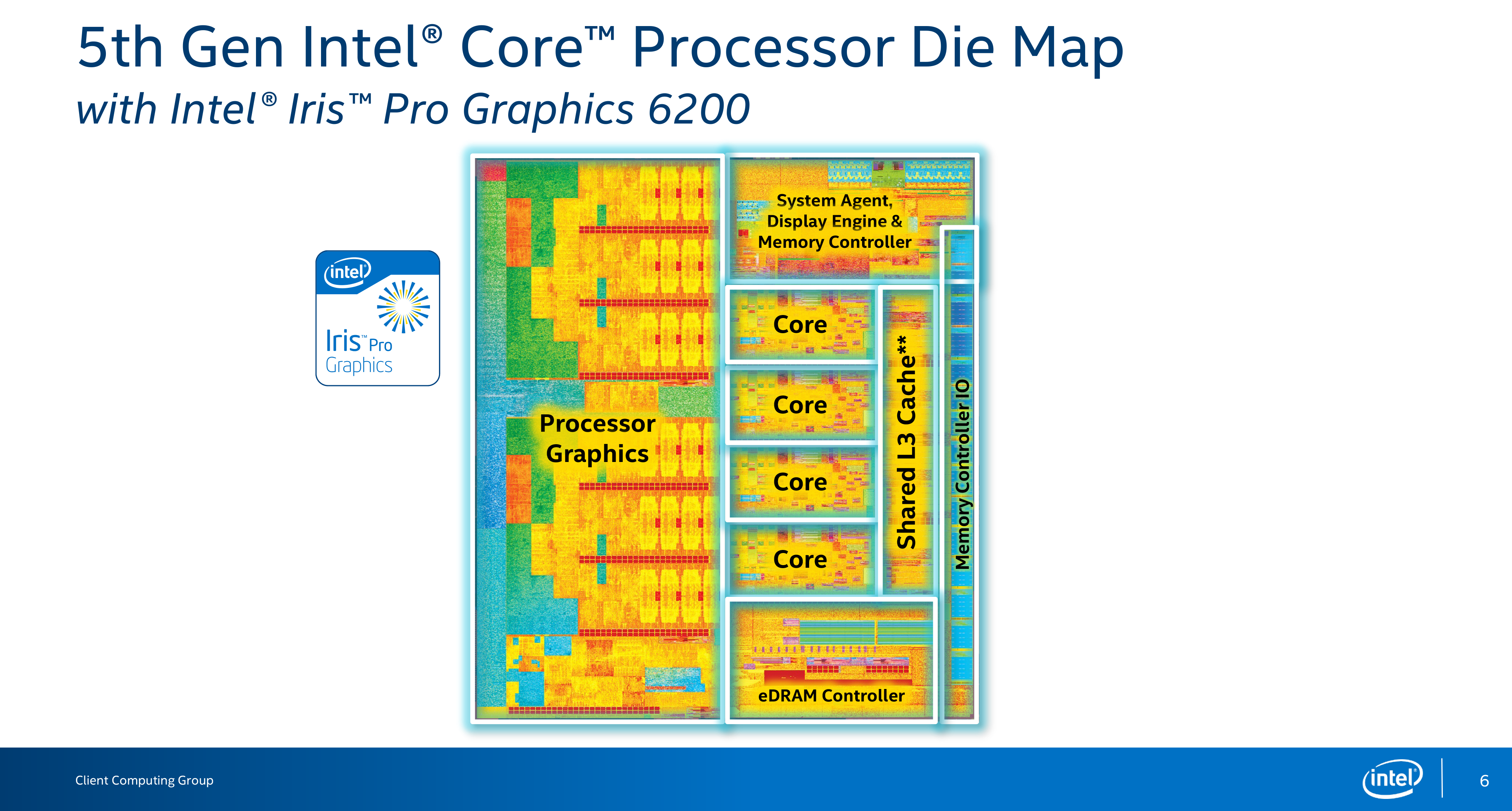
Broadwell-H Die Map
That brings us to today. All-told, Intel is launching ten different SKUs, five 47W laptop and five 65W 'desktop', using a mix of socketed (LGA) and soldered (BGA) parts. All five desktop SKUs are still technically Broadwell-H, and all five are 65W quad-core models featuring Intel's Iris Pro integrated graphics and the product's associated Crystal Well L4 cache. Meanwhile in an interesting turn of events, the two socketed models will be breaking the mold by becoming the first H-family processors to be socketed. These will be the parts we're looking at today.
The Effect of TDP
If we move back to those large processor stacks, Intel tends to produce a range of products from 15W TDP (extreme low power Xeon) through 35W, 55W and up to 84-88W for consumer then 160W for Xeon. Sticking with the consumer line for the moment, the high end overclocking models have recently sat in that 84-88W bracket, donning the i5-K or i7-K moniker and being some of the most talked about processors on forums and for custom builds. Broadwell changes this, and a lot of users might not expect it to.
Because the top Broadwell-DT SKUs are based on Intel's Broadwell-H design, both of the these SKUs ship with a TDP of 65W. As a result, frequencies on the cores are lower, and it means that these processors are best suited for comparison to 65W Haswell processors, such as the i7-4790S or i5-4590S, rather than the i7-4770K or i7-4790K. Thus users looking to upgrade their i5-K or i7-K might be wondering where their 84W processor is.
But both Broadwell-DT processors are overclockable, which adds an element of intrigue. I’ll speak specifically about the Crystal Well implementation in a second, but whether having that extra eDRAM on board effect overclocking is going to be a poignant question moving forward. If a 4.6 GHz Haswell user can also achieve 4.6 GHz on Broadwell, then the benefit of any IPC increase along with the eDRAM might be a driver for purchase. Unfortunately althugh both of the socketed chips are unlocked, due to both time constraints and severe pre-release firmware issues, we're going to have to save overclocking on Broadwell-DT for Part 2 of our coverage.
Integrated Graphics
Intel announced several months ago that Broadwell would be getting the first socketed processor with a Crystal Well implementation that would also be overclockable. For a number of us in the industry, this piqued our interest substantially. Crystal Well, Intel’s name for CPUs that carry extra eDRAM, offers the potential to alleviate DRAM pressure by acting as an L4 cache, but also gives more memory bandwidth for integrated graphics. Given that integrated graphics are typically memory starved to begin with, Crystal Well when announced was an interesting prospect. Unfortunately, for Haswell based models, Intel limited the project to soldered processors only, which meant there was no possible direct desktop comparison. This changes with Broadwell-DT.

Aside from this, in terms of integrated graphics only usage, Broadwell-DT has a full GT3e configuration of execution units that a Broadwell processor has been announced to have. On Core-M we see 24 EUs, Atom x7 with 16, Pentium/Celeron Broadwell-U has 12, while there are various models with 23 or 24 EUs in the Broadwell-U i3/i5 and i7 lines and a few Broadwell-U models with the full 48 EUs with Iris Pro 6100. There will be some Broadwell-H models with 48, which is the number that Broadwell-DT models with the designation ‘C’ or ‘R’ will have.
The current king of the socketed integrated graphics world is AMD’s A10-7870K, which we recently reviewed. Broadwell-DT with Crystal Well is going after that crown.


196 Comments
View All Comments
ppi - Wednesday, June 3, 2015 - link
Can G3260 run the latest games that require quad core CPU?wallysb01 - Tuesday, June 2, 2015 - link
What is ‘good enough’ performance though? I put a G3220 pentium in my wife’s computer and its plenty good enough for everything she does, which I suspect represents 99.8% of the population (Microsoft office stuff, email, facebook and Netflix/Amazon prime). Heck I can even play DOTA2 on it reasonably well.Intel has had ‘good enough’ graphics for damn near everyone for a while now and that G3220 was like $55 on sale. To me ‘good enough’ graphics isn’t playing modern games at high resolution and quick frame rates. If you want an iGPU to do that, you should expect to pay for it since you’re in the <0.1% of the population that cares.
Namisecond - Wednesday, June 3, 2015 - link
"Truth is (as pointed out) you can get an AMD chip with a $100 discrete graphics card which would blow either of the iGPUs away."Or you can compare that AMD chip and DGPU combo with an even cheaper Intel Pentium and same DGPU combo... :)
The_Assimilator - Wednesday, June 3, 2015 - link
Give it a generation or two - the cost of eDRAM will fall dramatically once Intel starts shipping it in millions of CPUs.Refuge - Tuesday, June 2, 2015 - link
They have proven they can build it, but at that price it is a bit of a moot point ATM.First lets see the price of these iGPU's come down before we count it a success.
ZeDestructor - Tuesday, June 2, 2015 - link
This who multipart review is slightly alarming...On the CPU itself: an IVB repeat: very minor CPU improvements, large GPU upgrade...
Oh, btw, since the CPUs are unlocked, can we get some identical speed benchmarks? Would be the nicest, easiest way to track IPC and eDRAM improvements.
Refuge - Tuesday, June 2, 2015 - link
The article mentioned them having problems with Beta Firmware stopping them from having overclocking and iGPU comparisons in this email.ZeDestructor - Wednesday, June 3, 2015 - link
I know. I feel that they should have pushed an early article out explaining the issues and published the review later on in one piece. You don't give good firmware, you get later coverage.vFunct - Tuesday, June 2, 2015 - link
The MSI page takeover ads here leave ZERO margins from the text..Ryan Smith - Tuesday, June 2, 2015 - link
On it. Sorry about that.