The Intel Broadwell Desktop Review: Core i7-5775C and Core i5-5675C Tested (Part 1)
by Ian Cutress on June 2, 2015 7:45 AM EST
On almost all PC technology forums, it is hard to escape users talking about what Intel’s next processor lineup will be. Due to initial yield issues in Intel’s 14nm node, Broadwell in both mobile and desktop ended up being delayed, somewhat substantially in the case of the desktop. So while motherboard manufacturers released their Z97 platform over 6 months ago, we have been waiting for Broadwell to arrive. That day is today, and we can lay the smackdown with some benchmark numbers too.
The Road to Broadwell
Broadwell, in its top level explanation, is the 14nm die shrink of Haswell which was built on 22nm. Using Intel’s 14nm process this results in a smaller silicon die and lower power consumption. Frequency will depend on the architecture and if the process is suited to frequency or power, but the CPU core underneath is still more-or-less Haswell, with some minor tweaks of course.
As part of Intel’s tick-tock strategy, this would be considered a tick:
| Intel's Tick-Tock Cadence | |||||
| Microarchitecture | Process Node | Tick or Tock | Release Year | ||
| Conroe/Merom | 65nm | Tock | 2006 | ||
| Penryn | 45nm | Tick | 2007 | ||
| Nehalem | 45nm | Tock | 2008 | ||
| Westmere | 32nm | Tick | 2010 | ||
| Sandy Bridge | 32nm | Tock | 2011 | ||
| Ivy Bridge | 22nm | Tick | 2012 | ||
| Haswell | 22nm | Tock | 2013 | ||
| Broadwell | 14nm | Tick | Core-M: 2014 Others: 2015 |
||
If history tells us anything, ticks are usually accompanied by small IPC increases, resulting in 5-10% better performance depending on the benchmark, but ultimately ticks still follow the same capabilities of the processor before them. Intel usually uses its ticks to introduce a new chipset with a large number of capabilities, which we saw with Z97 and its use of M.2/SATA Express on the chipset. If the classical idea of a three year cycle between upgrades is true, then back in the summer of 2012, we were playing around with Ivy Bridge, the tick to Sandy Bridge.
The Broadwell Launch
Back in mid 2014, Intel launched Core M, the first 14nm processor in the mass market and the first Broadwell based product. Core M is the official marketing designation for what was historically the Y series processor (Broadwell-Y), but Core M played a different role to other Y series processors. Core M brought the Core architecture down to a 4.5W thermal design, enabling small and thin fanless 2-in-1 laptop/tablet designs. When the first products started appearing around Christmas and CES, we tested a few and even got down and dirty with the questions that OEMs had to answer with their own chassis designs.
At CES (January 2015), Intel launched Broadwell-U. These devices are aimed more at traditional laptops, mini-PCs and all-in-ones, with the lower-wattage SKUs targeting devices in the 15W range. At the same time higher power 28W SKUs were also announced, with the graphics gamut migrating through the basic Gen 8 package up to Crystal Well based Iris Pro, using onboard EDRAM as an additional cache to improve graphics performance.

After Y and U in Intel’s naming scheme typically comes H, representing higher power (47W-65W) mobile processors or ones suitable for all-in-one type desktop replacement devices which are, for the most part, stationary. H processors are favorites in business due to their high performance, but typically these devices also require large batteries and can come with large (15-17”) screens. They are all soldered down parts as well. Technically some of the H processors are part of the launch today.
After Y, U and H is somewhat of a miasma. The processor lineup, depending on who you speak to, might be DT, S, T, or K. Some of these are also used in the processor names themselves, but we will use Broadwell-DT for consistency. Normally an Intel desktop processor lineup spans a gamut of SKUs, from Celerons, Pentiums, i3, i5 and up to i7. Some ranges consist of 50 or so SKUs, whereby one segment (i5/i7, for example) are launched first and the rest are launched later.
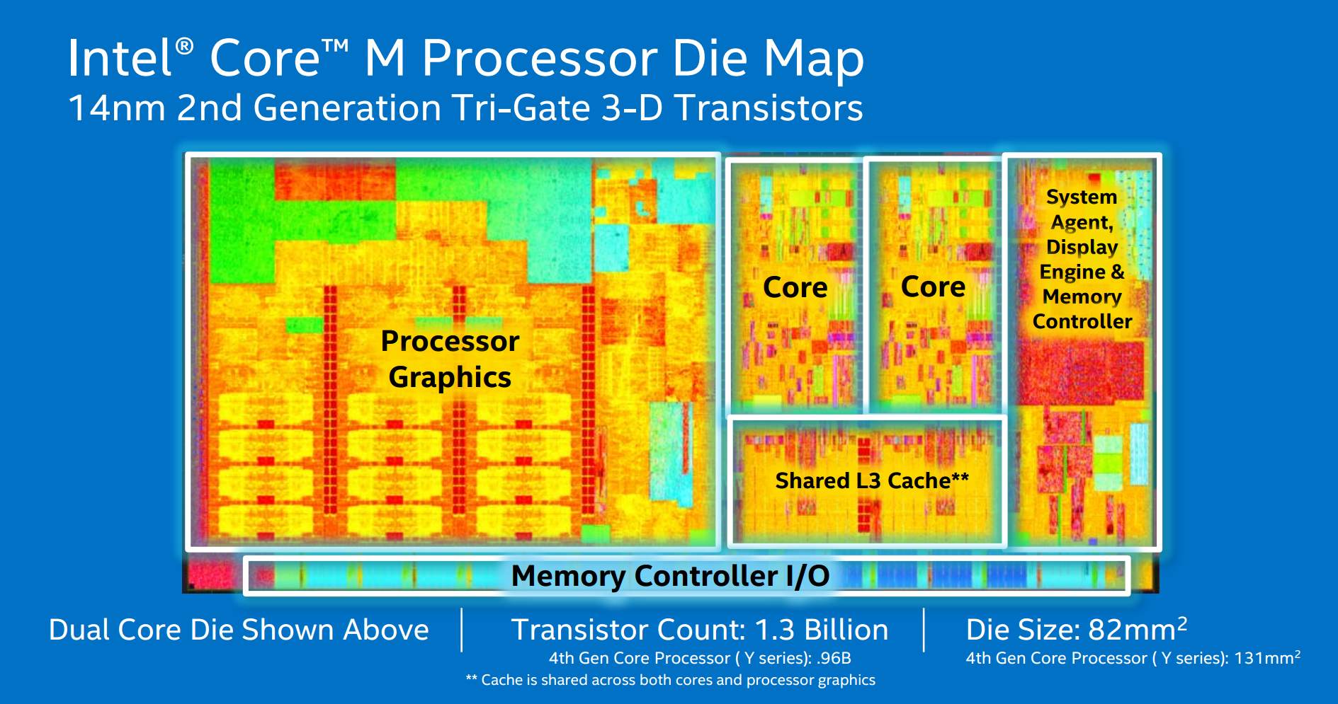
Broadwell-H Die Map
That brings us to today. All-told, Intel is launching ten different SKUs, five 47W laptop and five 65W 'desktop', using a mix of socketed (LGA) and soldered (BGA) parts. All five desktop SKUs are still technically Broadwell-H, and all five are 65W quad-core models featuring Intel's Iris Pro integrated graphics and the product's associated Crystal Well L4 cache. Meanwhile in an interesting turn of events, the two socketed models will be breaking the mold by becoming the first H-family processors to be socketed. These will be the parts we're looking at today.
The Effect of TDP
If we move back to those large processor stacks, Intel tends to produce a range of products from 15W TDP (extreme low power Xeon) through 35W, 55W and up to 84-88W for consumer then 160W for Xeon. Sticking with the consumer line for the moment, the high end overclocking models have recently sat in that 84-88W bracket, donning the i5-K or i7-K moniker and being some of the most talked about processors on forums and for custom builds. Broadwell changes this, and a lot of users might not expect it to.
Because the top Broadwell-DT SKUs are based on Intel's Broadwell-H design, both of the these SKUs ship with a TDP of 65W. As a result, frequencies on the cores are lower, and it means that these processors are best suited for comparison to 65W Haswell processors, such as the i7-4790S or i5-4590S, rather than the i7-4770K or i7-4790K. Thus users looking to upgrade their i5-K or i7-K might be wondering where their 84W processor is.
But both Broadwell-DT processors are overclockable, which adds an element of intrigue. I’ll speak specifically about the Crystal Well implementation in a second, but whether having that extra eDRAM on board effect overclocking is going to be a poignant question moving forward. If a 4.6 GHz Haswell user can also achieve 4.6 GHz on Broadwell, then the benefit of any IPC increase along with the eDRAM might be a driver for purchase. Unfortunately althugh both of the socketed chips are unlocked, due to both time constraints and severe pre-release firmware issues, we're going to have to save overclocking on Broadwell-DT for Part 2 of our coverage.
Integrated Graphics
Intel announced several months ago that Broadwell would be getting the first socketed processor with a Crystal Well implementation that would also be overclockable. For a number of us in the industry, this piqued our interest substantially. Crystal Well, Intel’s name for CPUs that carry extra eDRAM, offers the potential to alleviate DRAM pressure by acting as an L4 cache, but also gives more memory bandwidth for integrated graphics. Given that integrated graphics are typically memory starved to begin with, Crystal Well when announced was an interesting prospect. Unfortunately, for Haswell based models, Intel limited the project to soldered processors only, which meant there was no possible direct desktop comparison. This changes with Broadwell-DT.

Aside from this, in terms of integrated graphics only usage, Broadwell-DT has a full GT3e configuration of execution units that a Broadwell processor has been announced to have. On Core-M we see 24 EUs, Atom x7 with 16, Pentium/Celeron Broadwell-U has 12, while there are various models with 23 or 24 EUs in the Broadwell-U i3/i5 and i7 lines and a few Broadwell-U models with the full 48 EUs with Iris Pro 6100. There will be some Broadwell-H models with 48, which is the number that Broadwell-DT models with the designation ‘C’ or ‘R’ will have.
The current king of the socketed integrated graphics world is AMD’s A10-7870K, which we recently reviewed. Broadwell-DT with Crystal Well is going after that crown.


196 Comments
View All Comments
Shadowmaster625 - Tuesday, June 2, 2015 - link
Wow so anyone who buys one of these chips is spending half their money on a useless GPU that cant even beat a lowly R7 250. That is $120 to $180 totally wasted on GPU, which occupies half the die. Talk about a massive intel tax. What happens if intel only offer a K version that contains half the die wasted by this useless GPU? How many people are going to just suck it up and buy it even though half the chip will never be used because they will be running a real graphics card?TEAMSWITCHER - Tuesday, June 2, 2015 - link
These chips really only make sense for high end laptops like the 2015 MacBook Pro - which ironically doesn't use them. It boggles my mind that Intel is shipping so many transistors that go completely unused. It's the antithesis of Moore's Law - Intel silicon is HALF-USELESS.PubFiction - Wednesday, July 1, 2015 - link
That's because intel only cares about mobile now, this stuff isn't made for us its hacked to work for desktop users this stuff is all about mobile. Personally I deal with largely because I am just happy that people who buy stuff like macbooks can now actually have a chance of running boot camp and playing games. In the mobile work igpus have always been a big part of the scene. Also the better intel does with integrated graphics the more they are able to kill AMD/NVidia which is what they really want to do, slowly and steadily eat the bottom end of the GPU market out from under them. It used to be that ANY discreet graphics on a laptop was WAYYYYY better than integrated. But after intels 2nd gen core series the bottom X1XX and X2XX gpus seemed to not make any sense, and intel has been getting better to the point now that X4XXX gpus are starting to not make sense. This screws graphics makers into only being able to sell higher end X5XX + GPUs and they destroys their bread and butter money.bill.rookard - Tuesday, June 2, 2015 - link
As much as I hate to say it, I agree. While their new iGPU is beating AMDs iGPU, the place where such iGPUs make sense is in small HTPC scenarios most of all (apart from budget gaming laptops which have a completely different thermal restriction). The kicker is though that the pricing is far too high for even being considered for what amounts to a media playback machine. It's thermally too hot for a laptop scenario.If they had paired up the iGPU with a G3258 CPU core set and the Crystalwell DRAM, and priced it near AMD's offerings, THAT would be a very compelling product.
Refuge - Tuesday, June 2, 2015 - link
I'd buy that.extide - Tuesday, June 2, 2015 - link
Uhhh, maybe you need your eyes checked, but it is beating the R7 240 in all except one of the benchmarks...MikhailT - Tuesday, June 2, 2015 - link
Dude, go re-read the graphs, Intel is beating R7 in almost all benchmarks.Namisecond - Wednesday, June 3, 2015 - link
Actually, the GPU takes up over 60% of the die space on the first chips, there is a 2nd piece of silicon comprising the EDRAM that take up a not-so-insignificant piece of real estate on the chip.The situation with AMD APUs are similar, about 40-45% of their die space is GPU. When they go HBM, they will in a similar situation to Intel, and they'll need to charge much higher price to make up for the tech.
If you want lowest cost/value for CPU, get a Pentium, particularly the anniversary edition. They're cheap (I can get them for about $50) You can overclock the shit out of them and their IGPU only takes up about 40% of their die space. If you need more CPU power in the Socket 1150 format, get a Xeon E3 which has no IGPU...they are cheaper than Core I7, but they cost more than core I5.
der - Tuesday, June 2, 2015 - link
Awesome stuff! Killer chipset!der - Tuesday, June 2, 2015 - link
50th comment!