What Products Use Intel 10nm? SuperFin and 10++ Demystified
by Dr. Ian Cutress on September 25, 2020 9:00 AM EST_678x452.jpg)
For our audience that regularly keeps track of Intel’s product portfolio, it would be hard to miss that the naming strategy of Intel’s process node technologies is a bit of a mess. To some, those words are themselves an understatement, as Intel has shifted its naming strategy 2-3 times since the launch of Intel’s first 10nm products. Not only that, even Intel’s various departments internally have a hard time keeping track of ‘what is this manufacturing process being called today’ when the press like AnandTech ask for details on the latest upcoming products.
Knowing this, and knowing what issues Intel has been having, I wanted to demystify Intel’s manufacturing process naming scheme such that users and engineers alike, even if they are inside Intel, can understand what is what but also importantly why. The why is the crucial factor.
If you're looking for a handy decoder ring for Intel's 10nm Products, it's here in page 3.
Why Do We Have Multiple Versions of a Process?
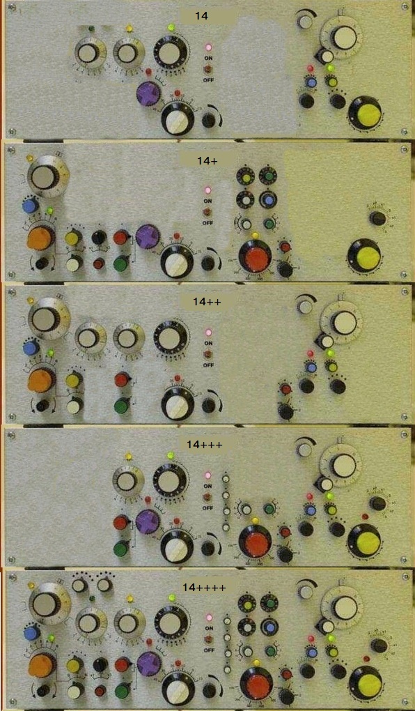
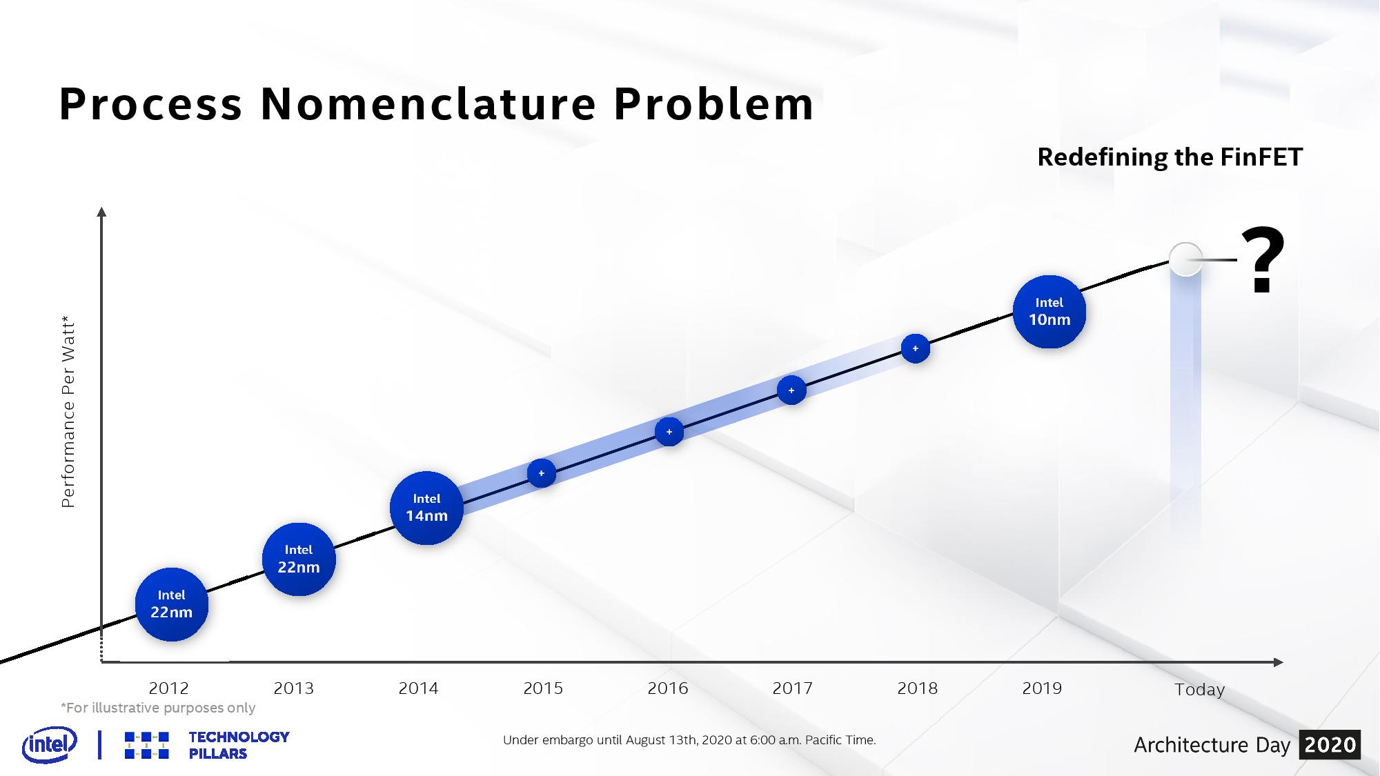
With Intel’s 14nm, we were invited to 14nm, 14+, 14++, 14+++, and if you believe Intel’s own slides, there were variants that went beyond this ++++ naming scheme. Each one of those additional + points on the end of the name signified a change in the process technology – usually to assist for increasing performance or efficiency.
Each one of these + points is an update to the BKM, or Best Known Methods.
While an engineer can draw an electrical layouts for a part of a processor, such as an addition circuit, actually applying that design to a silicon floorplan for manufacturing is a different skill altogether. Transistor libraries are designed to take advantage of a given process, and when a floorplan is optimized for a process, it can then be pasted and repeated as necessary – on top of this, simulation on thermals, power, and current density are applied to ensure that there are no hotspots or that critical paths inside the design have as few bottlenecks as possible.
When an update to the BKM occurs, two things can happen. Normally we see the update on the level of the transistor library that is changed – if the distance between two fins on a transistor increases for example, the transistor library and the macros may be made bigger, and then the floorplan might be redesigned to take account for this. As for any process node design, there are 100 different controls, and improving one might make three other controls worse, so it is a fine balancing act. Not only this, but the BKM has to be validated at the manufacturing level. The BKM update could apply to the metal stack as well, which in of itself can adjust the performance.
Lots of dials at each stage
In the long long past, BKM updates were never advertised externally. If Intel or TSMC or another foundry discovered a way to improve the performance, or decrease the voltage, or improve the yield, the update was silently rolled into the design and nothing much was made of it. Sometimes processors would be listed as ‘1.0 volts to 1.35 volts’, and it would just be a roll of the dice if a user obtained one of the lower voltage models.
However, as time between different process node updates has elongated, these BKM updates have started to be identified and effectively monetized by the semiconductor companies. An update to a process that improves the voltage by 50 millivolts and increases frequency by 200 MHz immediately becomes a productizable event, and products built on these updates can be offered for more money over the usual. Or, depending on the rate of updates, the whole next generation of products could be built on the update.

So we never saw BKM updates officially announced at Intel’s 45nm, 32nm, or 22nm process nodes. These updates were fast enough that the productization of any update didn’t warrant a full round of marketing. With 14nm, that changed.
Intel had discussed its roadmap beyond 14nm since its 2010 Investor Meeting. It predicted that the company would be on 14nm by 2013, 10nm by 2015, and 7nm by 2017. As we now know, 14nm was two years late, and 10nm was 2-4 years late. Because of the introduction of 10nm being delayed, Intel decided to productize its 14nm BKM updates, and signified those with + points.
Intel’s current official line is that there have been four updates to 14nm, creating five ‘generations’.
More Plus Means More Meme
Because of all the + points, Intel’s marketing sometimes getting it wrong, and perhaps a little bit of ‘++’ in most programming languages meaning ‘+1’, the whole concept of adding + to the process node has become a meme – a meme at Intel’s expense, purely on the basis of its failure to deliver 10nm before the 14++++ naming scheme got out of hand.


143 Comments
View All Comments
dotjaz - Friday, September 25, 2020 - link
You are so delusional. They don't have that many nodes. Process improves all the time, but some improvements require no change on the design front, some requires a simple re-spin, some require design changes to take advantage of design rule changes.The ones requiring no re-spin is not a new node at all, because those are generally counted as yield improvements.
Spunjji - Friday, September 25, 2020 - link
Most of these improvements were already acknowledged by Intel, though not always named. The delusion is yours.drexnx - Friday, September 25, 2020 - link
Devil's Canyon wasn't a process change, it was a TIM change and package cap changeSkylake was just 14
Coffee and Coffee refresh are both 14++
Spunjji - Friday, September 25, 2020 - link
Pretty sure they rolled in unannounced changes, too. Check the voltage requirements / binning. They used to do that quietly all the time back then.RSAUser - Saturday, September 26, 2020 - link
I just realized I have never owned a 14nm product till end of 2019 as a laptop, i7 950, i5 4460, i7 4720HQ, i7 4790, and those lasted till I got this i7 9750H as AMD 4000's hadn't been released yet, desktops are 3600X and 3900X.Kind of crazy how well those CPU's stood the test of time, since I remember before my 950 upgrading about every 1.5 years.
szabikopy - Friday, September 25, 2020 - link
Is the table on the 3rd page 100% legit?I’m asking because I’m not sure if intel mentioned that Alder lake will be manufactured on 10ESF.
If they did (and I just didn’t capture) then I’m more than a happy person. I just hope the next gen golden cove + 10 ESF will be great
Ahsan Qureshi - Friday, September 25, 2020 - link
Yes. Alder Lake, Sapphire Rapids and Xe-HP will be manufactured on 10nmESF.Machinus - Friday, September 25, 2020 - link
Ok, but when will they actually sell desktop chips? 10nm++++, according to your chart?Intel has become a broken clock. Tick-tok-tok-tok-tok...
dotjaz - Friday, September 25, 2020 - link
But the original article about Atom still says 10SF. If it's indeed 10nm Mark II or 10+ as originally named, then where did the 10++ come from?soaringrocks - Friday, September 25, 2020 - link
The problem is that line width of 14nm, 10nm, 7nm, etc. is a lousy way to describe Fab processes. It's worse than Apples vs. Oranges, it's more like Apples vs. Orangutans. Seeing people get overly hyped on process steps is just plain stupid. Look at the benchmarks for the apps you care about, that's all that really matters.