The Apple iPad Pro Review
by Ryan Smith, Joshua Ho & Brandon Chester on January 22, 2016 8:10 AM ESTSoC Analysis: Apple A9X
Diving into the heart of the iPad Pro, we have Apple’s latest generation tablet SoC, A9X. Like the other Apple X series SoCs before it, A9X is by and large an enhanced and physically larger version of Apple’s latest phone SoC, taking advantage of the greater space and heat dissipation afforded by a tablet to produce a more powerful SoC.

Apple's A9X (Image Courtesy iFixit)
That Apple has developed a new SoC to launch alongside the iPad Pro is in no way surprising, but just as how the iPad Pro has ramifications for the overall iPad lineup as Apple gets into the productivity tablet market, iPad Pro’s genesis is reflected in its component selection. Apple already needed a powerful SoC for the iPad Air 2 in order to keep performance up with the tablet’s high resolution of the screen, and iPad Pro in turn pushes Apple’s performance needs even harder. Not only is there an even higher resolution screen to drive – the 2732x2048 display has about 66% of the pixels of a 4K display – but now Apple needs to deliver suitable performance for content creation and meaningful multitasking. I don’t want to imply that the A9X was somehow specifically designed from scratch for the iPad Pro, as there are a number of more important engineering considerations, but I do want to highlight how the iPad Pro is not just another iPad, and that as Apple expands the capabilities of the iPad they need to expand the performance as well if they wish to extend their reputation for smooth UX performance.
Looking at the specifications of the A9X, it seems like Apple always throws us a curveball on the X series SoCs, and for their latest SoC this is no different. With A8X Apple delivered more RAM on a wider memory bus, a larger GPU, and surprisingly, three Typhoon CPU cores. To date it’s still not clear just why Apple went with three CPU cores on A8X – was it for multitasking, or as an alternative means to boost performance – and A9X’s configuration only serves to highlight this enigma.
| Apple SoC Comparison | ||||||
| A9X | A9 | A8X | A6X | |||
| CPU | 2x Twister | 2x Twister | 3x Typhoon | 2x Swift | ||
| CPU Clockspeed | 2.26GHz | 1.85GHz | 1.5GHz | 1.3GHz | ||
| GPU | PVR 12 Cluster Series7XT | PVR 6 Cluster Series7 (PVR GT7600) |
PVR 8 Cluster Series6XT (APL GXA6850) |
PVR SGX554 MP4 | ||
| RAM | 4GB LPDDR4 | 2GB LPDDR4 | 2GB LPDDR3 | 1GB LPDDR2 | ||
| Memory Bus Width | 128-bit | 64-bit | 128-bit | 128-bit | ||
| Memory Bandwidth | 51.2GB/sec | 25.6GB/sec | 25.6GB/sec | 17.1GB/sec | ||
| L2 Cache | 3MB | 3MB | 2MB | 1MB | ||
| L3 Cache | None | 4MB | 4MB | N/A | ||
| Manufacturing Process | TSMC 16nm FinFET | TSMC 16nm & Samsung 14nm |
TSMC 20nm | Samsung 32nm | ||
Instead of continuing with a triple-core CPU design for A9X, for their latest X series SoC Apple has dropped back down to just a pair of Twister CPU cores. The catch here – and why two cores is in many ways better than three – is that relative to A8X and A9, Apple has cranked up their CPU clockspeeds. Way, way up. Whereas the iPad Air 2 (A8X) shipped at 1.5GHz and the iPhone 6s (A9) at 1.85GHz, the A9X sees Apple push their clockspeed to 2.26GHz. Not counting the architectural changes, this is 22% higher clocked than the A9 and 51% higher than the A8X.
The fact that Apple dropped back down to 2 CPU cores is unexpected given that we don’t expect Apple to ever go backwards in such a fashion, and while we’ll never know the official reason for everything Apple does, in retrospect I’m starting to think that A8X was an anomaly and Apple didn’t really want a tri-core CPU in the first place. A8X came at a time where Apple was bound by TSMC’s 20nm process and couldn’t drive up their clockspeeds without vastly increasing power consumption, so a third core was a far more power effective option.
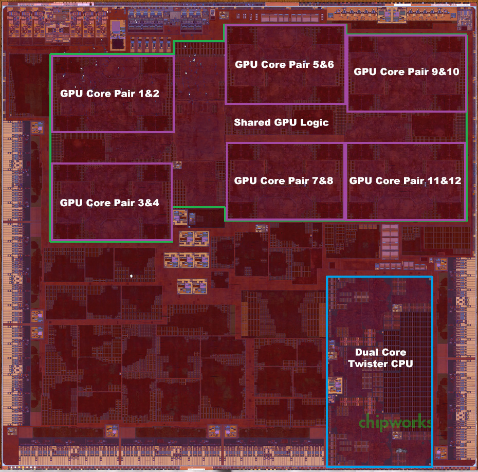
A9X Die Shot w/AT Annotations (Die Shot Courtesy Chipworks)
Overall this means that iPad Pro and A9X will set a very high bar for tablet CPU performance. As we’ve already seen in the iPhone 6s review, the Twister CPU core is very potent and in most cases faster than any other ARM CPU core by leaps and bounds. Cranking up the clockspeed a further 22% only serves to open up that gap even further, as Twister is now reaching clockspeeds similar to the likes of Cortex-A57 and A72, but with its much wider execution pipeline and greater IPC. This is also the reason that an Intel Core CPU comparison is so interesting, as Intel’s tablet-class Core processors in many ways are the target to beat on overall CPU performance, and we’ll be touching upon this subject in greater detail a bit later.
GPU: Imagination PowerVR 12 Cluster Series 7XT
Meanwhile on the GPU side, as expected Apple has further increased the number of clusters on their SoC to drive the higher resolution display of a tablet. Whereas A9 used a 6 cluster design (PVR GT7600), A9X doubles this, giving us a relatively massive 12 cluster design.
In Imagination’s PowerVR Series7XT roadmap, the company doesn’t have an official name for a 12 cluster configuration, as this falls between the 8 cluster GT7800 and 16 cluster GT7900. So for the moment I’m simply calling it a “PowerVR 12 cluster Series7XT design,” and with any luck Imagination will use a more fine-grained naming scheme for future generations of PowerVR graphics.
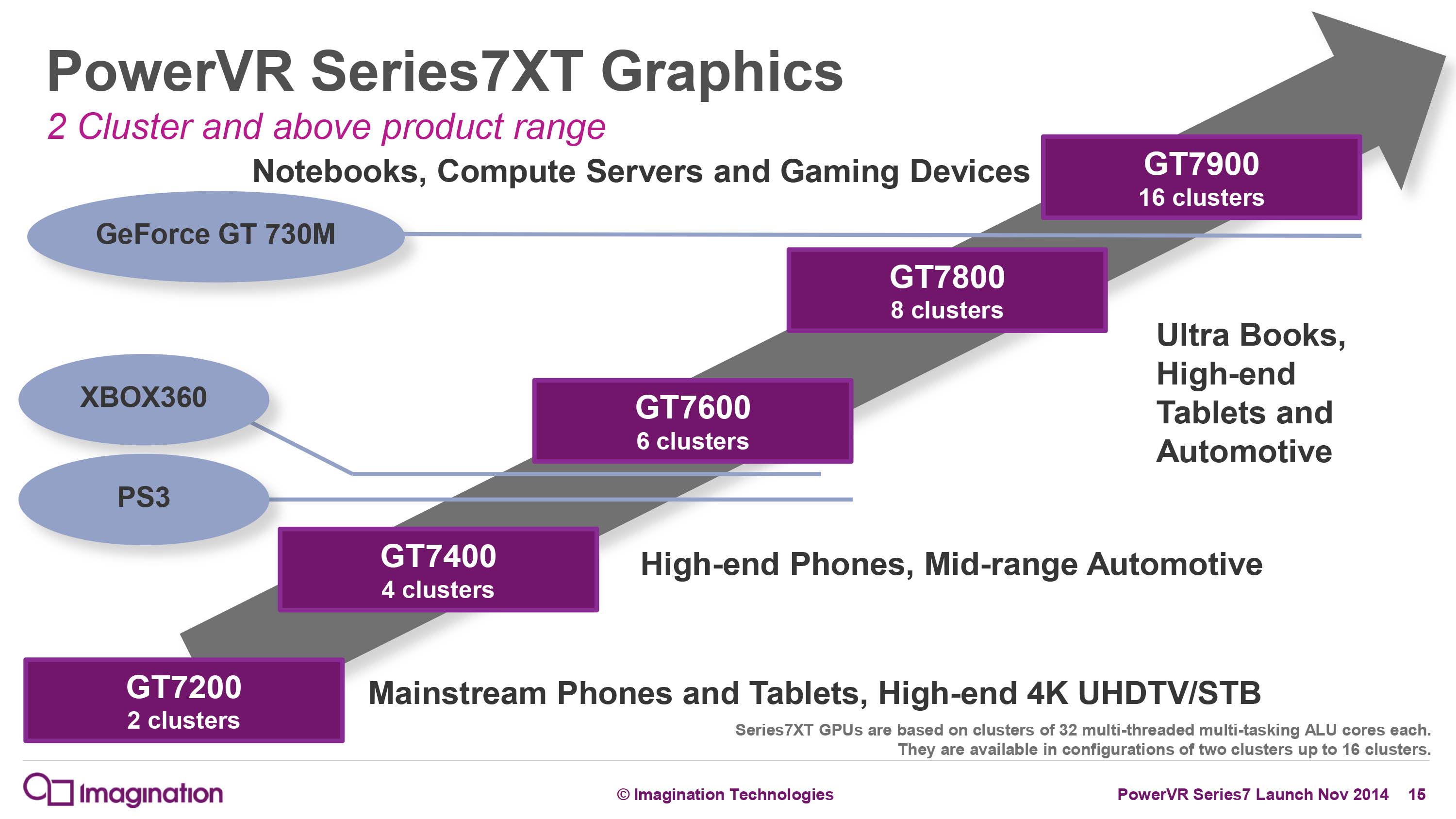
In any case, the use of a 12 cluster design is a bit surprising from an engineering standpoint since it means that Apple was willing to take the die space hit to implement additional GPU clusters, despite the impact this would have on chip yields and costs. If anything, with the larger thermal capacity and battery of the iPad Pro, I had expected Apple to use higher GPU clockspeeds (and eat the power cost) in order to save on chip costs. Instead what we’re seeing is a GPU that essentially offers twice the GPU power of A9’s GPU.
However to put all of this in context, keep in mind that iPad Pro’s display is 5.95Mpixels, versus the 2.07Mpixel screen on the iPhone 6s Plus. So although Apple has doubled the number of GPU clusters for A9X – and I suspect clocked it fairly similarly – that increased performance will be very quickly consumed by the iPad Pro’s high resolution screen. Consequently even a 12 cluster GPU design is something of a compromise; if Apple wanted to maintain the same level of GPU performance per pixel as in the iPhone 6s family, they would have needed an even more powerful GPU. Which just goes to show how demanding tablets can be.
Memory Subsystem: 128-bit LPDDR4-3200, No L3 Cache
Responsibility for feeding the beast that is A9X’s GPU falls to A9X’s 128-bit LPDDR4 memory controller configuration. With twice as many GPU clusters, Apple needs twice as much memory bandwidth to maintain the same bandwidth-to-core ratio, so like the past X-series tablet SoCs, A9X implements a 128-bit bus. For Apple this means they now have a sizable 51.2GB/sec of memory bandwidth to play with. For an SoC this is a huge amount of bandwidth, but at the same time it’s quickly going to be consumed by those 12 GPU clusters.
| Geekbench 3 Memory Bandwidth Comparison (1 thread) | ||||||
| Stream Copy | Stream Scale | Stream Add | Stream Triad | |||
| Apple A9X 2.26GHz | 20.8 GB/s | 15.0 GB/s | 15.3 GB/s | 15.1 GB/s | ||
| Apple A8X 1.5GHz | 14.2 GB/s | 7.44 GB/s | 7.54 GB/s | 7.49 GB/s | ||
| A9X Advantage | 46.4% | 101% | 103% | 102% | ||
It’s also while looking at A9X’s memory subsystem however that we find our second and final curveball for A9X: the L3 cache. Or rather, the lack thereof. For multiple generations now Apple has used an L3 cache on both their phone and tablet SoCs to help feed both the CPU and GPU, as even a fast memory bus can’t keep up with a low latency local cache. Even as recent as A9, Apple included a 4MB victim cache. However for A9X there is no L3 cache; the only caches on the chip are the individual L1 and L2 caches for the CPU and GPU, along with some even smaller amounts for cache for various other functional blocks..
The big question right now is why Apple would do this. Our traditional wisdom here is that the L3 cache was put in place to service both the CPU and GPU, but especially the GPU. Graphics rendering is a memory bandwidth-intensive operation, and as Apple has consistently been well ahead of many of the other ARM SoC designers in GPU performance, they have been running headlong into the performance limitations imposed by narrow mobile memory interfaces. An L3 cache, in turn, would alleviate some of that memory pressure and keep both CPU and GPU performance up.
One explanation may be that Apple deemed the L3 cache no longer necessary with the A9X’s 128-bit LPDDR4 memory bus; that 51.2GB/sec of bandwidth meant that they no longer needed the cache to avoid GPU stalls. However while the use of LPDDR4 may be a factor, Apple’s ratio of bandwidth-to-GPU cores of roughly 4.26GB/sec-to-1 core is identical to A9’s, which does have an L3 cache. With A9X being a larger A9 in so many ways, this alone isn’t the whole story.
What’s especially curious is that the L3 cache on the A9 wasn’t costing Apple much in the way of space. Chipworks puts the size of A9’s 4MB L3 cache block at a puny ~4.5 mm2, which is just 3% the size of A9X. So although there is a cost to adding L3 cache, unless there are issues we can’t see even with a die shot (e.g. routing), Apple didn’t save much by getting rid of the L3 cache.
Our own Andrei Frumusanu suspects that it may be a power matter, and that Apple was using the L3 cache to save on power-expensive memory operations on the A9. With A9X however, it’s a tablet SoC that doesn’t face the same power restrictions, and as a result doesn’t need a power-saving cache. This would be coupled with the fact that with double the GPU cores, there would be a lot more pressure on just a 4MB cache versus the pressure created by A9, which in turn may drive the need for a larger cache and ultimately an even larger die size.
As it stands there’s no one obvious reason, and it’s likely that all 3 factors – die size, LPDDR4, and power needs – all played a part here, with only those within the halls of One Infinite Loop knowing for sure. However I will add that since Apple has removed the L3 cache, the GPU L2 cache must be sizable. Imagination’s tile based deferred rendering technology needs an on-chip cache to hold tiles in to work on, and while they don’t need an entire frame’s worth of cache (which on iPad Pro would be over 21MB), they do need enough cache to hold a single tile. It’s much harder to estimate GPU L2 cache size from a die shot (especially with Apple’s asymmetrical design), but I wouldn’t be surprised of A9X’s GPU L2 cache is greater than A9’s or A8X’s.
Building A9X Big: 147mm2, Manufactured By TSMC
Finally, let’s talk about the construction and fabrication of the A9X SoC itself. Chipworks’ previous analysis shows that the A9X is roughly 147mm2 in die size, and that it’s manufactured by TSMC on their 16nm FinFET process.
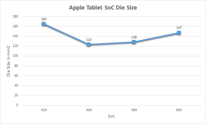
At 147mm2 the A9X is the second-largest of Apple’s X-series tablet SoCs. Only the A5X, the first such SoC, was larger. Fittingly, it was also built relative to Apple’s equally large A5 phone SoC. With only 3 previous tablet SoCs to use as a point of comparison I’m not sure there’s really a sweet spot we can say that Apple likes to stick to, but after two generations of SoCs in the 120mm2 to 130mm2 range, A9X is noticeably larger.
Some of that comes from the fact that A9 itself is a bit larger than normal – the TSMC version is 104.5mm2 – but Apple has also clearly added a fair bit to the SoC. The wildcard here is what yields look like for Apple, as that would tell us a lot about whether a 147mm2 A9X is just a large part or if Apple has taken a greater amount of risk than usual here.
A9X continues to be the largest 16nm FinFET ASIC we know to be in mass production at TSMC (we’ll ignore FPGAs for now), and while this will undoubtedly change a bit later this year once the next-generation discrete GPUs come online, I don’t think you’ll find a better example of how the contract chip manufacturing market has changed in a single generation. 4 years ago it would be GPUs leading the charge, but now it’s phone SoCs and a rather sizable tablet SoC that are first out of the gate. After almost a decade of catching up, SoCs have now reached the bleeding edge for chip fabrication, enabling rapid performance growth, but also inheriting the risks of being the leader. I won’t dwell on this too much, but I’m immensely curious about both what A9X yields are like as the largest FinFET ASIC at TSMC, and just how much of TSMC’s FinFET capacity Apple has been consuming with the production of A9 and A9X.
Finally, it's also interesting to note just how large A9X is compared to other high performance processors. Intel's latest-generation Skylake processors measure in at ~99mm2 for the 2 core GT2 configuration (Skylake-Y 2+2), and even the 4 core desktop GT2 configuration (Intel Skylake-K 4+2) is only 122mm2. So A9X is larger than either of these CPU cores, though admittedly as a whole SoC A9X contains a number of functional units either not present on Skylake or on Skylake's Platform Controller Hub (PCH). Still, this is the first time that we've seen an Apple launch a tablet SoC larger than an Intel 4 core desktop CPU.


408 Comments
View All Comments
ghostbit - Friday, January 22, 2016 - link
I like iPads as thin clients.wolfemane - Friday, January 22, 2016 - link
The article was a great read and very thorough. Thank you Joshua Ho, Brandon Chester & Ryan Smith. I look forward to the next article!nrencoret - Saturday, January 23, 2016 - link
It seems cliché in Apple product reviews to mention bias, but this article fits the cliché quite well.The selective comparisons with other tablets are alarming. As others pointed out, no other product with a stylus has been thoroughly reviewed. A bare mention of the SP3 pen is all we get whilst all of the cons explored in the stylus section have no counterpoint as to how strong Surface tablets (and even Samsung devices) are at note taking (the exporting woes with the iPad come to mind). Even more troubling is the keyboard section where anyone who has decent tech knowledge knows how big of an improvement is the SP4 keyboard just to have it conveniently ignored in the conversation. The section is even worse when one considers the lack of angle adjustments, stability issues and cumbersome setup of the iPad keyboard are compared to the SP. Not to say a thing about the lack of mouse input which makes the whole desktop use uncomfortable. Finally the bland treatment given to the charge time of the tablet is inexcusable.
On the plus side, the SOC section is impeccable.
But the overall falling (as with all of Joshua's Apple writings) is a self-fulfilling prophecy: he likes the iPad and excuses or dismisses the the product's failings and conveniently never discusses what other products+software do better. Happy you like your iPad and you've written a good essay as to why its a good device for you, but this, a professional unbiased review its not.
10101010 - Saturday, January 23, 2016 - link
As a Note 8 and 12.2 owner, I can say the "exporting woes" of the iPad Pro are absolutely trivial in comparison. Samsung completely fumbled building a pen app ecosystem. This will not be the case with the iPad Pro.When it comes to the Surface Pro, we need to talk about how Windows is a broken platform and few developers want to write apps for it anymore. Even Microsoft's own developers don't like Windows anymore and are writing their latest software for other platforms using open source frameworks such as Electron.
Let's not forget to mention that the Surface Pro hardware, firmware, and drivers are so flaky that there is "SurfaceGate":
https://www.thurrott.com/mobile/microsoft-surface/...
And we also have the endless "whack-a-mole" adventure that is trying to maintain some semblance of data privacy/security with Windows 10 and its factory installed malware and forced updates.
One could on. You know, so things are more "professionally unbiased".
royalcrown - Sunday, January 31, 2016 - link
Thank you, for I am racing this on a Note 12.2 now. The S Pens have good hardware but their size sucks and the apps for them are too dumbed down or too many steps just to take simple notes.name99 - Saturday, January 23, 2016 - link
Hmm. For a team that is supposedly so blindly in love with Apple, they seem remarkably ignorant about how to actually DO things. For example, here's how you export those Pencil written notes:you install an iOS app called PrinterPro https://readdle.com/products/printerpro OR
https://itunes.apple.com/us/app/printer-pro-print-...
This installs a share sheet into iOS which allows you to "print" to a variety of real or virtual printers. One of these virtual printers is, of course, a PDF printer which just create a PDF file.
THIS sort of thing is why Apple folks get so irritated with Windows/Linux folks. You keep claiming that something or other cannot be done (on OSX or iOS) but 95% of the time your actual complaint is "I don't know how to do ... on OSX/iOS; therefore obviously it can't be done because I know everything in the universe about computing". There's more than one way to do things, folks, and just because the Windows way is some weird voodoo of "install a driver; go into some dialog that hasn't been updated since Windows 95; change three settings in the registry; now you can create PDFs" doesn't mean that iOS makes you do the same thing if you want to create PDFs.
Share sheets are the generic inter-app communication mechanism for iOS, and anyone who was actually familiar with the platform would immediately think that this was the sort of place to look to solve the problem.
As for Printer Pro being "unsupported". Well, my version is actually free because Apple liked the product so much they sponsored it being free on the app store for two weeks or so. I don't think they're likely to yank it from the store...
Should this be part of the OS? Well, plenty of thing should be part of every OS. How long did it take WINDOWS to get a Print to PDF option?...
My guess is that at some point it will be wrapped into the standard iOS bundle of features, but that right now Apple have higher priorities, and the third party solution works very well without the sorts of security, stability, or power concerns that might compel Apple to move other features into the base OS more rapidly.
royalcrown - Sunday, January 31, 2016 - link
True, but it'seems stupid in this day of very common WiFi printers that you can'take just install an app from the app store that is from the printer manufacturer that allows IOS to print directly (No Airprint nonsense). How a out the fact that it took until IOS 8 or 9 to attach a PDF to an email.I like both companies and use both, but this is the kind of stupid crap that apple does that gives haters a "Foot in the door". It's why I switched out my IPad 3 for a Note at the time.
bitbank - Saturday, January 23, 2016 - link
Small correction to your comparison of ARM to x86 ISA: you said "By comparison, the ARM ISA has no direct equivalent to this instruction. Any instruction like leal/leaq is going to take multiple instructions.". This is incorrect. ARM with its 3-operand instructions usually takes fewer instructions compared to Intel. In this case, there is a single instruction which is more powerful than the Intel equivalent -> ADD R1,R2,R3,LSL #2. This is effectively R1 = R2 + 4*R3. The barrel shifter and 3-operand instructions mean you can do more work than the Intel ISA allows. Individual ARM instructions are on average longer than Intel instructions, but you usually need fewer of them to accomplish the same task.JoshHo - Saturday, January 23, 2016 - link
Fiora Aeterna has also helpfully pointed this out. I've since updated the article to resolve this inaccuracy and use a (hopefully) better example.name99 - Sunday, January 24, 2016 - link
We can be more precise about this. Experiments have been done about the density of code and it is a fact that ARM-v8 is very slightly DENSER than x64 code. ARM-v7 was slightly less dense than 32-bit x86 code.The barrel shifter is not relevant to ARM-v8 (neither is predication). What is relevant is a very cleverly designed ISA that actually exploits what we've learned about usual code patterns over the past 30 years or so. So ARM has load and store register pair, or just enough predication-like instructions (CSEL and the concatenated branch conditions), or a way to distinguish between instructions that do and don't set branch conditions, or an encoding of literals that is, as matter of empirical reality, substantially denser than a flat encoding. All these make for a substantially denser ISA than the traditional load-store type ISA of something like MIPS or POWER.