Original Link: https://www.anandtech.com/show/17047/the-intel-12th-gen-core-i912900k-review-hybrid-performance-brings-hybrid-complexity
The Intel 12th Gen Core i9-12900K Review: Hybrid Performance Brings Hybrid Complexity
by Dr. Ian Cutress & Andrei Frumusanu on November 4, 2021 9:00 AM ESTToday marks the official retail availability of Intel’s 12th Generation Core processors, starting with the overclockable versions this side of the New Year, and the rest in 2022. These new processors are the first widescale launch of a hybrid processor design for mainstream Windows-based desktops using the underlying x86 architecture: Intel has created two types of core, a performance core and an efficiency core, to work together and provide the best of performance and low power in a singular package. This hybrid design and new platform however has a number of rocks in the river to navigate: adapting Windows 10, Windows 11, and all sorts of software to work properly, but also introduction of DDR5 at a time when DDR5 is still not widely available. There are so many potential pitfalls for this product, and we’re testing the flagship Core i9-12900K in a few key areas to see how it tackles them.
Let’s Talk Processors
Since August, Intel has been talking about the design of its 12th Generation Core processor family, also known as Alder Lake. We’ve already detailed over 16000 words on the topic, covering the fundamentals of each new core, how Intel has worked with Microsoft to improve Windows performance with the new design, as features like DDR5, chipsets, and overclocking. We’ll briefly cover the highlights here, but these two articles are worth the read for those that want to know.
- Intel Architecture Day 2021: Alder Lake, Golden Cove, and Gracemont Detailed
- Intel 12th Gen Core Alder Lake for Desktops: CPUs, Chipsets, Power, DDR5, OCh
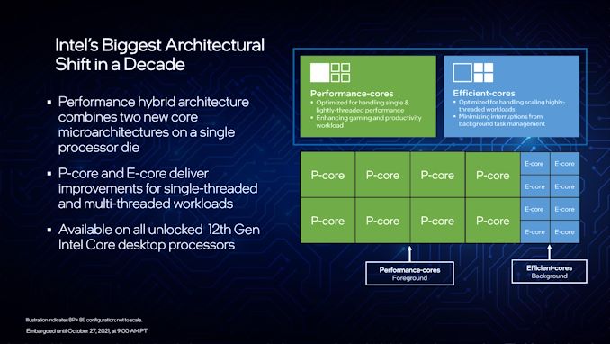
At the heart of Intel’s processors is a hybrid, or heterogeneous, core design. The desktop processor silicon will have eight performance cores (P-cores) and eight efficiency cores (E-cores), the latter in two groups of four. Each of the cores is designed differently to optimize for their targets, but supports the same software. The goal is that software that is not urgent runs on efficiency cores, but time-sensitive software runs on performance cores, and that has required a new management control between the processor and Windows has been developed to enable Alder Lake to work at its best. That control is fully enabled in Windows 11, and Windows 10 can get most of the way there but doesn’t have all the bells and whistles for finer details – Linux support is in development.
The use of this hybrid design makes some traditional performance measurements difficult to compare. Intel states that individually the performance cores are +19% over 11th Generation, and the efficiency cores are around 10th Generation performance levels at much lower power. At peak performance Intel has showcased in slides that four E-cores will outperform two 6th Generation cores in both performance and power, with the E-core being optimized also for performance per physical unit of silicon. Alternatively, Intel can use all P-cores and all E-cores on a singular task, up to 241W for the Core i9 processor.
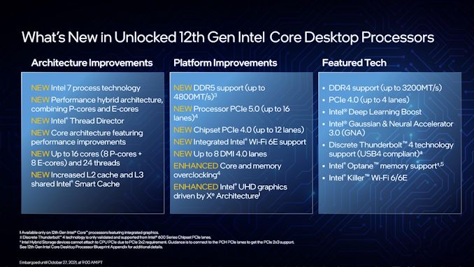
On top of all this, Intel is bringing new technology into the mix with 12th Gen Core. These processors will have PCIe 5.0 support, but also DDR5-4800 and DDR4-3200 support on the memory. This means that Alder Lake motherboards, using the new LGA1700 socket and Z690 chipsets, will be either DDR4 or DDR5 compatible. No motherboard will have slots for both (they’re not interchangeable), but as we are quite early in the DDR5 lifecycle, getting a DDR4 motherboard might be the only way for users to get hold of an Alder Lake system using their current memory. We test both DDR4 and DDR5 later on in the review to see if there is a performance difference.
A small word on power (see this article for more info) – rather than giving a simple ‘TDP’ value as in previous generations, which only specified the power at a base frequency, Intel is expanding to providing both a Base power and a Turbo power this time around. On top of that, Intel is also making these processors have ‘infinite Turbo time’, meaning that with the right cooling, users should expect these processors to run up to the Turbo power indefinitely during heavy workloads. Intel giving both numbers is a welcome change, although some users have criticized the decreasing turbo power for Core i7 and Core i5.
As we reported last week, here are the processors shipping today:
| Intel 12th Gen Core, Alder Lake | |||||||||
| AnandTech | Cores P+E/T |
E-Core Base |
E-Core Turbo |
P-Core Base |
P-Core Turbo |
IGP | Base W |
Turbo W |
Price $1ku |
| i9-12900K | 8+8/24 | 2400 | 3900 | 3200 | 5200 | 770 | 125 | 241 | $589 |
| i9-12900KF | 8+8/24 | 2400 | 3900 | 3200 | 5200 | - | 125 | 241 | $564 |
| i7-12700K | 8+4/20 | 2700 | 3800 | 3600 | 5000 | 770 | 125 | 190 | $409 |
| i7-12700KF | 8+4/20 | 2700 | 3800 | 3600 | 5000 | - | 125 | 190 | $384 |
| i5-12600K | 6+4/16 | 2800 | 3600 | 3700 | 4900 | 770 | 125 | 150 | $289 |
| i5-12600KF | 6+4/16 | 2800 | 3600 | 3700 | 4900 | - | 125 | 150 | $264 |
Processors that have a K are overclockable, and those with an F do not have integrated graphics. The graphics on each of the non-F chips are Xe-LP graphics, the same as the previous generation.
At the top of the stack is the Core i9-12900K, with eight P-cores and eight E-cores, running at a maximum 241 W. Moving down to i7 gives eight P-cores and four E-cores at 190 W, and the Core i5 gives six P-cores and four E-cores at 150 W. We understand that future processors may have six P-core and zero E-core designs.
| Compare at $550+ | |||||||
| AnandTech | Cores P+E/T |
P-Core Base |
P-Core Turbo |
IGP | Base W |
Turbo W |
Price |
| R9 5950X | 16/32 | 3400 | 4900 | - | 105 | 142 | $799 |
| i9-12900K | 8+8/24 | 3200 | 5200 | 770 | 125 | 241 | $589* |
| R9 5900X | 12/24 | 3700 | 4800 | - | 105 | 142 | $549 |
| * AMD Quotes RRP, Intel quotes 'tray' as 1000-unit sales. Retail is ~$650 | |||||||
The Core i9-12900K, the focus of this review today, is listed at a tray price of $589. Intel always lists tray pricing, which means ‘price if you buy 1000 units as an OEM’. The retail packaging is often another +5-10% or so, which means actual retail pricing will be nearer $650, plus tax. At that pricing it really sits between two competitive processors: the 16-core Ryzen 9 5950X ($749) and the 12-core Ryzen 9 5900X ($549).
Let’s Talk Operating Systems
Suffice to say, from the perspective of a hardware reviewer, this launch is a difficult one to cover. Normally with a new processor we would run A vs B, and that’s most of the data we need aside from some specific edge cases. For this launch, there are other factors to consider:
- P-core vs E-core
- DDR5 vs DDR4
- Windows 11 vs Windows 10
Every new degree of freedom to test is arguably a doubling of testing, so in this case 23 means 8x more testing than a normal review. Fun times. But the point to drill down to here is the last one.
Windows 11 is really new. So new in fact that performance issues on various platforms are still being fixed: recently a patch was put out to correct an issue with AMD L3 cache sizes, for example. Even when Intel presented data against AMD last week, it had to admit that they didn’t have the patch yet. Other reviewers have showcased a number of performance consistency issues with the OS when simply changing CPUs in the same system. The interplay of a new operating system that may improve performance, combined with a new heterogeneous core design, combined with new memory, and limited testing time (guess who’s CPUs were held in customs for a week), means that for the next few weeks, or months, we’re going to be seeing new performance numbers and comparisons crop up.
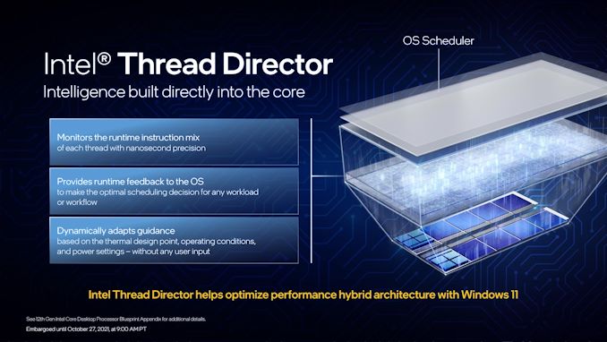
From Intel’s perspective, Windows 11 brings the full use of its Thread Director technology online. Normally the easiest way to run software on a CPU is to assume all the cores are the same - the advent of hyperthreading, favoured core, and other similar features meant that add-ins were applied to the operating system to help it work as intended at the hardware level. Hybrid designs add much more complexity, and so Intel built a new technology called Thread Director to handle it. At the base level, TD understands the CPU in terms of performance per core but also efficiency per core, and it can tell P-core from E-core from favoured P-core from a hyperthread. It gathers all this information, and tells the operating system what it knows – which threads need performance, what threads it thinks needs efficiency, and what are the best candidates to move up or down that stack. The operating system is still king, and can choose to ignore what TD suggests, but Windows 11 can take all that data and make decisions depending on what the user is currently focused on, the priority level of those tasks, and additional software hooks from developers regarding priority and latency.
The idea is that with Windows 11, it all works. With Windows 10, it almost all works. The main difference Intel told us is although Windows 10 can separate cores apart, and hyperthreads, it doesn’t really understand efficiency that well. So its decisions are made more in regards to performance requirements, rather than performance vs efficiency. At the end of the day, all this should mean to the user is that Windows 10 tries to minimizes the run-to-run variation, but Windows 11 does it better. Ultimate best-case performance shouldn’t change in any serious way: a single thread on a P-core, or across several P-cores for example, should perform the same.
Let’s Talk Testing
This review is going to focus on these specific comparisons:
- Core i9-12900K on DDR5 vs the Competition
- Core i9-12900K on DDR5 vs Core i9-12900K on DDR4
- Power and Performance of the P-Core vs E-Core
- Core i9-12900K Windows 11 vs Windows 10
Normally when a new version of Windows is launched, I stay as far away from it as possible. On a personal level, I enjoy consistency and stability in my workflow, but also when it comes to reviewing hardware – being able to be confident in having a consistent platform is the only true way to draw meaningful conclusions over a sustained period. Nonetheless, when a new operating system is launched, there is always the call to bulk wholesale move testing to a new platform. Windows 11 is Windows 10 with a new dress and some details moved around and improved, so it should be easier than most, however I’m still going to wait until the bulk of those initial early adopter issues, especially those that might affect performance are solved, before performing a flat refresh of our testing ecosystem. Expect that to come in Q2 next year, where we will also be updating to NVMe testing, and soliciting updates for benchmarks and new tests to explore.
For our testing, we’re leveraging the following platforms:
| Alder Lake Test Systems | ||
| AnandTech | DDR5 | DDR4 |
| CPU | Core i9-12900K 8+8 Cores, 24 Threads 125W Base, 241W Turbo |
|
| Motherboard | MSI Z690 Unify | MSI Z690 Carbon Wi-Fi |
| Memory | SK Hynix 2x32 GB DDR5-4800 CL40 |
ADATA 2x32 GB DDR4-3200 CL22 |
| Cooling | MSI Coreliquid 360mm AIO |
Corsair H150i Elite 360mm AIO |
| Storage | Crucial MX500 2TB | |
| Power Supply | Corsair AX860i | |
| GPUs | Sapphire RX460 2GB (Non-Gaming Tests) NVIDIA RTX 2080 Ti (Gaming Tests), Driver 496.49 |
|
| Operating Systems | Windows 10 21H1 Windows 11 Up to Date Ubuntu 21.10 (for SPEC Power) |
|
All other chips for comparison were ran as tests listed in our benchmark database, Bench, on Windows 10.
Highlights of this review
- The new P-core is faster than a Zen 3 core, and uses 55-65 W in ST
- The new E-core is faster than Skylake, and uses 11-15 W in ST
- Maximum all-core power recorded was 272 W, but usually below 241 W (even in AVX-512)
- Despite Intel saying otherwise, Alder Lake does have AVX-512 support (if you want it)!
- Overall Performance of i9-12900K is well above i9-11900K
- Performance against AMD overall is a mixed bag: win on ST, MT varies
- Performance per Watt of the P-cores still lags Zen3
- There are some fundamental Windows 10 issues (that can be solved)
- Don’t trust thermal software just yet, it says 100C but it’s not
- Linux idle power is lower than Windows idle power
- DDR5 gains shine through in specific MT tests, otherwise neutral to DDR4
Intel Disabled AVX-512, but Not Really
One of the more interesting disclosures about Alder Lake earlier this year is that the processor would not have Intel’s latest 512-bit vector extensions, AVX-512, despite the company making a big song and dance about how it was working with software developers to optimize for it, why it was in their laptop chips, and how no transistor should be left behind. One of the issues was that the processor, inside the silicon, actually did have the AVX-512 unit there. We were told as part of the extra Architecture Day Q&A that it would be fused off, and the plan was for all Alder Lake CPUs to have it fused off.
Part of the issue of AVX-512 support on Alder Lake was that only the P-cores have the feature in the design, and the E-cores do not. One of the downsides of most operating system design is that when a new program starts, there’s no way to accurately determine which core it will be placed on, or if the code will take a path that includes AVX-512. So if, naively, AVX-512 code was run on a processor that did not understand it, like an E-core, it would cause a critical error, which could cause the system to crash. Experts in the area have pointed out that technically the chip could be designed to catch the error and hand off the thread to the right core, but Intel hasn’t done this here as it adds complexity. By disabling AVX-512 in Alder Lake, it means that both the P-cores and the E-cores have a unified common instruction set, and they can both run all software supported on either.
There was a thought that if Intel were to release a version of Alder Lake with P-cores only, or if a system had all the E-cores disabled, there might be an option to have AVX-512. Intel shot down that concept almost immediately, saying very succinctly that no Alder Lake CPU would support AVX-512.
Nonetheless, we test to see if it is actually fused off.
On my first system, the MSI motherboard, I could easily disable the E-cores. That was no problem, just adjust the BIOS to zero E-cores. However this wasn’t sufficient, as AVX-512 was still clearly not detected.
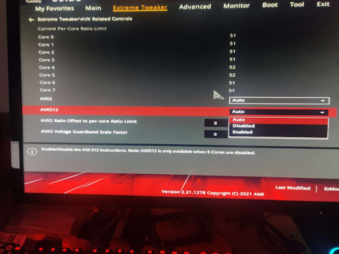
On a second system, an ASUS motherboard, there was some funny option in the BIOS.
Well I’ll be a monkey’s uncle. There’s an option, right there, front and centre for AVX-512. So we disable the E-cores and enable this option. We have AVX-512 support.
For those that have some insight into AVX-512 might be aware that there are a couple of dozen different versions/add-ons of AVX-512. We confirmed that the P-cores in Alder Lake have:
- AVX512-F / F_X64
- AVX512-DQ / DQ_X64
- AVX512-CD
- AVX512-BW / BW_X64
- AVX512-VL / VLBW / VLDQ / VL_IFMA / VL_VBMI / VL_VNNI
- AVX512_VNNI
- AVX512_VBMI / VBMI2
- AVX512_IFMA
- AVX512_BITALG
- AVX512_VAES
- AVX512_VPCLMULQDQ
- AVX512_GFNI
- AVX512_BF16
- AVX512_VP2INTERSECT
- AVX512_FP16
This is, essentially, the full Sapphire Rapids AVX-512 support. That makes sense, given that this is the same core that’s meant to be in Sapphire Rapids (albeit with cache changes). The core also supports dual AVX-512 ports, as we’re detecting a throughput of 2 per cycle on 512-bit add/subtracts.
For performance, I’m using our trusty 3DPMAVX benchmark here, and compared to the previous generation Rocket Lake (which did have AVX-512), the score increases by a few percent in a scenario which isn’t DRAM limited.
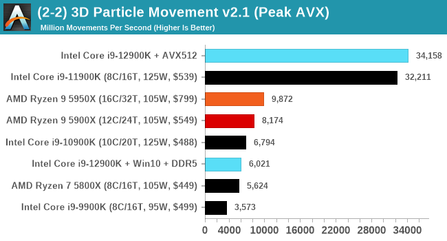
Now back in that Rocket Lake review, we noted that the highest power consumption observed for the chip was during AVX-512 operation. At that time, our testing showcased a big +50W jump between AVX2 and AVX-512 workloads. This time around however, Intel has managed to adjust the power requirements for AVX-512, and in our testing they were very reasonable:
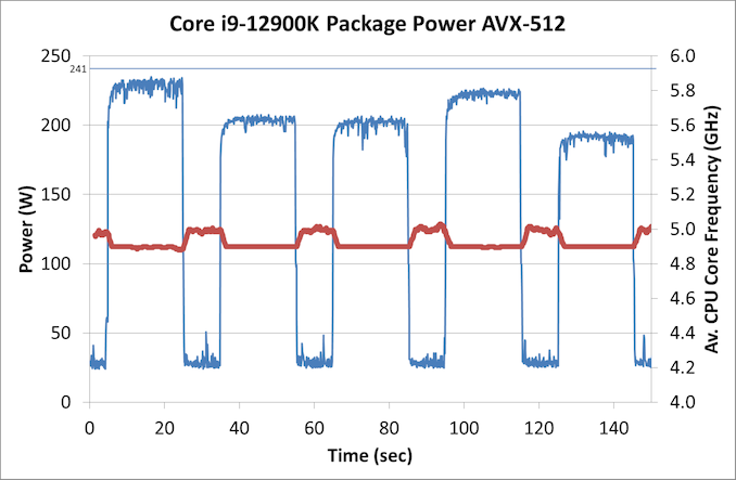
In this graph, we’re showing each of the 3DPM algorithms running for 20 seconds, then idling for 10 seconds. Each one has a different intensity of AVX-512, hence why the power is up and down. IN each instance, the CPU used an all-core turbo frequency of 4.9 GHz, in line with non-AVX code, and our peak power observed is actually 233 W, well below the 241 W rated for processor turbo.
Why?
So the question then refocuses back on Intel. Why was AVX-512 support for Alder Lake dropped, and why were we told that it is fused off, when clearly it isn’t?
Based on a variety of conversations with individuals I won’t name, it appears that the plan to have AVX-512 in Alder Lake was there from the beginning. It was working on early silicon, even as far as ES1/ES2 silicon, and was enabled in the firmware. Then for whatever reason, someone decided to remove that support from Intel’s Plan of Record (POR, the features list of the product).
By removing it from the POR, this means that the feature did not have to be validated for retail, which partly speeds up the binning and testing/validation process. As far as I understand it, the engineers working on the feature were livid. While all their hard work would be put to use on Sapphire Rapids, it still meant that Alder Lake would drop the feature and those that wanted to prepare for Alder Lake would have to remain on simulated support. Not only that, as we’ve seen since Architecture Day, it’s been a bit of a marketing headache. Whoever initiated that dropped support clearly didn’t think of how that messaging was going to down, or how they were going to spin it into a positive. For the record, removing support isn’t a positive, especially given how much hullaballoo it seems to have caused.
We’ve done some extensive research on what Intel has done in order to ‘disable’ AVX-512. It looks like that in the base firmware that Intel creates, there is an option to enable/disable the unit, as there probably is for a lot of other features. Intel then hands this base firmware to the vendors and they adjust it how they wish. As far as we understand, when the decision to drop AVX-512 from the POR was made, the option to enable/disable AVX-512 was obfuscated in the base firmware. The idea is that the motherboard vendors wouldn’t be able to change the option unless they specifically knew how to – the standard hook to change that option was gone.
However, some motherboard vendors have figured it out. In our discoveries, we have learned that this works on ASUS, GIGABYTE, and ASRock motherboards, however MSI motherboards do not have this option. It’s worth noting that all the motherboard vendors likely designed all of their boards on the premise that AVX-512 and its high current draw needs would be there, so when Intel cut it, it meant perhaps that some boards were over-engineered with a higher cost than needed. I bet a few weren’t happy.
Update: MSI reached out to me and have said they will have this feature in BIOS versions 1.11 and above. Some boards already have the BIOS available, the rest will follow shortly.
But AVX-512 is enabled, and we are now in a state of limbo on this. Clearly the unit isn’t fused off, it’s just been hidden. Some engineers are annoyed, but other smart engineers at the motherboard vendors figured it out. So what does Intel do from here?
First, Intel could put the hammer down and execute a scorched earth policy. Completely strip out the firmware for AVX-512, and dictate that future BIOS/UEFI releases on all motherboards going forward cannot have this option, lest the motherboard manufacturer face some sort of wrath / decrease in marketing discretionary funds / support. Any future CPUs coming out of the factory would actually have the unit fused out, rather than simply turned off.
Second, Intel could lift the lid, acknowledge that someone made an error, and state that they’re prepared to properly support it in future consumer chips with proper validation when in a P-core only mode. This includes the upcoming P-core only chips next year.
Third, treat it like overclocking. It is what it is, your mileage may vary, no guarantee of performance consistency, and any errata generated will not be fixed in future revisions.
As I’ve mentioned, apparently this decision didn’t go down to well. I’m still trying to find the name of the person/people who made this decision, and get their side of the story as to technically why this decision was made. We were told that ‘No Transistor Left Behind’, except these ones in that person’s mind, clearly.
Fundamental Windows 10 Issues: Priority and Focus
In a normal scenario the expected running of software on a computer is that all cores are equal, such that any thread can go anywhere and expect the same performance. As we’ve already discussed, the new Alder Lake design of performance cores and efficiency cores means that not everything is equal, and the system has to know where to put what workload for maximum effect.
To this end, Intel created Thread Director, which acts as the ultimate information depot for what is happening on the CPU. It knows what threads are where, what each of the cores can do, how compute heavy or memory heavy each thread is, and where all the thermal hot spots and voltages mix in. With that information, it sends data to the operating system about how the threads are operating, with suggestions of actions to perform, or which threads can be promoted/demoted in the event of something new coming in. The operating system scheduler is then the ring master, combining the Thread Director information with the information it has about the user – what software is in the foreground, what threads are tagged as low priority, and then it’s the operating system that actually orchestrates the whole process.
Intel has said that Windows 11 does all of this. The only thing Windows 10 doesn’t have is insight into the efficiency of the cores on the CPU. It assumes the efficiency is equal, but the performance differs – so instead of ‘performance vs efficiency’ cores, Windows 10 sees it more as ‘high performance vs low performance’. Intel says the net result of this will be seen only in run-to-run variation: there’s more of a chance of a thread spending some time on the low performance cores before being moved to high performance, and so anyone benchmarking multiple runs will see more variation on Windows 10 than Windows 11. But ultimately, the peak performance should be identical.
However, there are a couple of flaws.
At Intel’s Innovation event last week, we learned that the operating system will de-emphasise any workload that is not in user focus. For an office workload, or a mobile workload, this makes sense – if you’re in Excel, for example, you want Excel to be on the performance cores and those 60 chrome tabs you have open are all considered background tasks for the efficiency cores. The same with email, Netflix, or video games – what you are using there and then matters most, and everything else doesn’t really need the CPU.
However, this breaks down when it comes to more professional workflows. Intel gave an example of a content creator, exporting a video, and while that was processing going to edit some images. This puts the video export on the efficiency cores, while the image editor gets the performance cores. In my experience, the limiting factor in that scenario is the video export, not the image editor – what should take a unit of time on the P-cores now suddenly takes 2-3x on the E-cores while I’m doing something else. This extends to anyone who multi-tasks during a heavy workload, such as programmers waiting for the latest compile. Under this philosophy, the user would have to keep the important window in focus at all times. Beyond this, any software that spawns heavy compute threads in the background, without the potential for focus, would also be placed on the E-cores.
Personally, I think this is a crazy way to do things, especially on a desktop. Intel tells me there are three ways to stop this behaviour:
- Running dual monitors stops it
- Changing Windows Power Plan from Balanced to High Performance stops it
- There’s an option in the BIOS that, when enabled, means the Scroll Lock can be used to disable/park the E-cores, meaning nothing will be scheduled on them when the Scroll Lock is active.
(For those that are interested in Alder Lake confusing some DRM packages like Denuvo, #3 can also be used in that instance to play older games.)
For users that only have one window open at a time, or aren’t relying on any serious all-core time-critical workload, it won’t really affect them. But for anyone else, it’s a bit of a problem. But the problems don’t stop there, at least for Windows 10.
Knowing my luck by the time this review goes out it might be fixed, but:
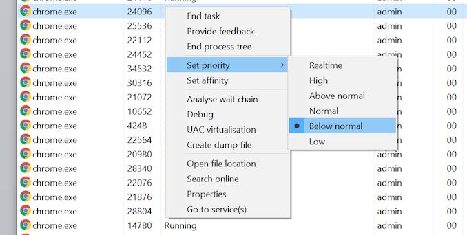
Windows 10 also uses the threads in-OS priority as a guide for core scheduling. For any users that have played around with the task manager, there is an option to give a program a priority: Realtime, High, Above Normal, Normal, Below Normal, or Idle. The default is Normal. Behind the scenes this is actually a number from 0 to 31, where Normal is 8.
Some software will naturally give itself a lower priority, usually a 7 (below normal), as an indication to the operating system of either ‘I’m not important’ or ‘I’m a heavy workload and I want the user to still have a responsive system’. This second reason is an issue on Windows 10, as with Alder Lake it will schedule the workload on the E-cores. So even if it is a heavy workload, moving to the E-cores will slow it down, compared to simply being across all cores but at a lower priority. This is regardless of whether the program is in focus or not.
Of the normal benchmarks we run, this issue flared up mainly with the rendering tasks like CineBench, Corona, POV-Ray, but also happened with yCruncher and Keyshot (a visualization tool). In speaking to others, it appears that sometimes Chrome has a similar issue. The only way to fix these programs was to go into task manager and either (a) change the thread priority to Normal or higher, or (b) change the thread affinity to only P-cores. Software such as Project Lasso can be used to make sure that every time these programs are loaded, the priority is bumped up to normal.
Power: P-Core vs E-Core, Win10 vs Win11
For Alder Lake, Intel brings two new things into the mix when we start talking about power.
First is what we’ve already talked about, the new P-core and E-core, each with different levels of performance per watt and targeted at different sorts of workloads. While the P-cores are expected to mimic previous generations of Intel processors, the E-cores should offer an interesting look into how low power operation might work on these systems and in future mobile systems.
The second element is how Intel is describing power. Rather than simply quote a ‘TDP’, or Thermal Design Power, Intel has decided (with much rejoicing) to start putting two numbers next to each processor, one for the base processor power and one for maximum turbo processor power, which we’ll call Base and Turbo. The idea is that the Base power mimics the TDP value we had before – it’s the power at which the all-core base frequency is guaranteed to. The Turbo power indicates the highest power level that should be observed in normal power virus (usually defined as something causing 90-95% of the CPU to continually switch) situation. There is usually a weighted time factor that limits how long a processor can remain in its Turbo state for slowly reeling back, but for the K processors Intel has made that time factor effectively infinite – with the right cooling, these processors should be able to use their Turbo power all day, all week, and all year.
So with that in mind, let’s start simply looking at the individual P-cores and E-cores.
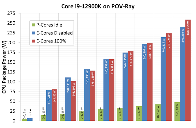
Listed in red, in this test, all 8P+8E cores fully loaded (on DDR5), we get a CPU package power of 259 W. The progression from idle to load is steady, although there is a big jump from idle to single core. When one core is loaded, we go from 7 W to 78 W, which is a big 71 W jump. Because this is package power (the output for core power had some issues), this does include firing up the ring, the L3 cache, and the DRAM controller, but even if that makes 20% of the difference, we’re still looking at ~55-60 W enabled for a single core. By comparison, for our single thread SPEC power testing on Linux, we see a more modest 25-30W per core, which we put down to POV-Ray’s instruction density.
By contrast, in green, the E-cores only jump from 5 W to 15 W when a single core is active, and that is the same number as we see on SPEC power testing. Using all the E-cores, at 3.9 GHz, brings the package power up to 48 W total.
It is worth noting that there are differences between the blue bars (P-cores only) and the red bars (all cores, with E-cores loaded all the time), and that sometimes the blue bar consumes more power than the red bar. Our blue bar tests were done with E-cores disabled in the BIOS, which means that there might be more leeway in balancing a workload across a smaller number of cores, allowing for higher power. However as everything ramps up, the advantage swings the other way it seems. It’s a bit odd to see this behavior.
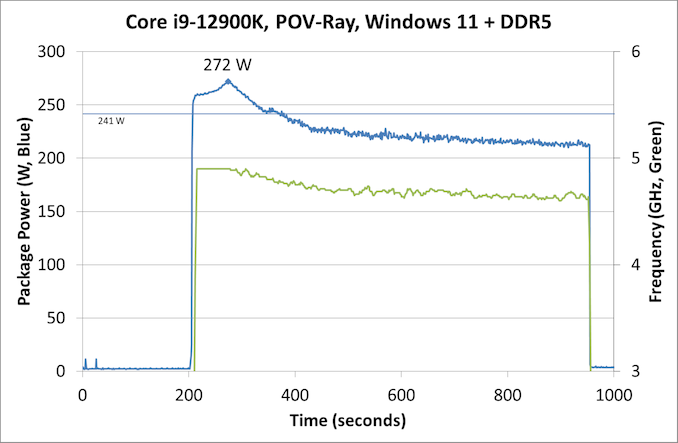
Moving on to individual testing, and here’s a look at a power trace of POV-Ray in Windows 11:
Here we’re seeing a higher spike in power, up to 272 W now, with the system at 4.9 GHz all-core. Interestingly enough, we see a decrease of power through the 241 W Turbo Power limit, and it settles around 225 W, with the reported frequency actually dropping to between 4.7-4.8 GHz instead. Technically this all-core is meant to take into account some of the E-cores, so this might be a case of the workload distributing itself and finding the best performance/power point when it comes to instruction mix, cache mix, and IO requirements. However, it takes a good 3-5 minutes to get there, if that’s the case.
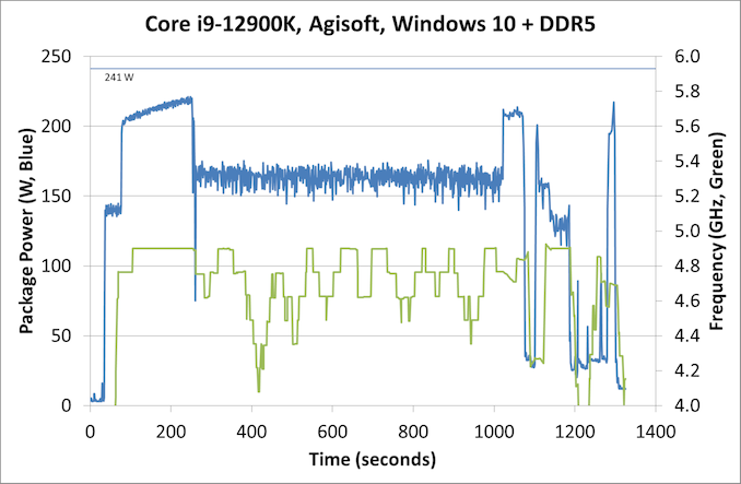
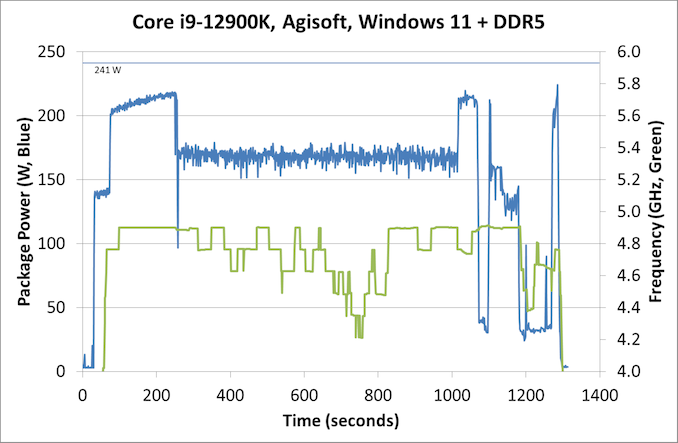
Intrigued by this, I looked at how some of our other tests did between different operating systems. Enter Agisoft:
Between Windows 10 and Windows 11, the traces look near identical. The actual run time was 5 seconds faster on Windows 11 out of 20 minutes, so 0.4% faster, which we would consider run-to-run variation. The peaks and spikes look barely higher in Windows 11, and the frequency trace in Windows 11 looks a little more consistent, but overall they’re practically the same.
For our usual power graphs, we get something like this, and we’ll also add in the AVX-512 numbers from that page:
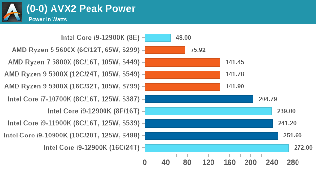
Compared to Intel’s previous 11th Generation Processor, the Alder Lake Core i9 uses more power during AVX2, but is actually lower in AVX-512. The difficulty of presenting this graph in the future is based on those E-cores; they're more efficient, and as you’ll see in the results later. Even on AVX-512, Alder Lake pulls out a performance lead using 50 W fewer than 11th Gen.
When we compare it to AMD however, with that 142 W PPT limit that AMD has, Intel is often trailing at a 20-70 W deficit when we’re looking at full load efficiency. That being said, Intel is likely going to argue that in mixed workloads, such as two software programs running where something is on the E-cores, it wants to be the more efficient design.
Instruction Changes
Both of the processor cores inside Alder Lake are brand new – they build on the previous generation Core and Atom designs in multiple ways. As always, Intel gives us a high level overview of the microarchitecture changes, as we’ve written in an article from Architecture Day:
At the highest level, the P-core supports a 6-wide decode (up from 4), and has split the execution ports to allow for more operations to execute at once, enabling higher IPC and ILP from workflow that can take advantage. Usually a wider decode consumes a lot more power, but Intel says that its micro-op cache (now 4K) and front-end are improved enough that the decode engine spends 80% of its time power gated.
For the E-core, similarly it also has a 6-wide decode, although split to 2x3-wide. It has a 17 execution ports, buffered by double the load/store support of the previous generation Atom core. Beyond this, Gracemont is the first Atom core to support AVX2 instructions.
As part of our analysis into new microarchitectures, we also do an instruction sweep to see what other benefits have been added. The following is literally a raw list of changes, which we are still in the process of going through. Please forgive the raw data. Big thanks to our industry friends who help with this analysis.
Any of the following that is listed as A|B means A in latency (in clocks) and B in reciprocal throughput (1/instructions).
P-core: Golden Cove vs Cypress Cove
Microarchitecture Changes:
- 6-wide decoder with 32b window: it means code size much less important, e.g. 3 MOV imm64 / clks;(last similar 50% jump was Pentium -> Pentium Pro in 1995, Conroe in 2006 was just 3->4 jump)
- Triple load: (almost) universal
- every GPR, SSE, VEX, EVEX load gains (only MMX load unsupported)
- BROADCAST*, GATHER*, PREFETCH* also gains
- Decoupled double FADD units
- every single and double SIMD VADD/VSUB (and AVX VADDSUB* and VHADD*/VHSUB*) has latency gains
- Another ADD/SUB means 4->2 clks
- Another MUL means 4->3 clks
- AVX512 support: 512b ADD/SUB rec. throughput 0.5, as in server!
- exception: half precision ADD/SUB handled by FMAs
- exception: x87 FADD remained 3 clks
- Some form of GPR (general purpose register) immediate additions treated as NOPs (removed at the "allocate/rename/move ellimination/zeroing idioms" step)
- LEA r64, [r64+imm8]
- ADD r64, imm8
- ADD r64, imm32
- INC r64
- Is this just for 64b addition GPRs?
- eliminated instructions:
- MOV r32/r64
- (V)MOV(A/U)(PS/PD/DQ) xmm, ymm
- 0-5 0x66 NOP
- LNOP3-7
- CLC/STC
- zeroing idioms:
- (V)XORPS/PD, (V)PXOR xmm, ymm
- (V)PSUB(U)B/W/D/Q xmm
- (V)PCMPGTB/W/D/Q xmm
- (V)PXOR xmm
Faster GPR instructions (vs Cypress Cove):
- LOCK latency 20->18 clks
- LEA with scale throughput 2->3/clk
- (I)MUL r8 latency 4->3 clks
- LAHF latency 3->1 clks
- CMPS* latency 5->4 clks
- REP CMPSB 1->3.7 Bytes/clock
- REP SCASB 0.5->1.85 Bytes/clock
- REP MOVS* 115->122 Bytes/clock
- CMPXVHG16B 20|20 -> 16|14
- PREFETCH* throughput 1->3/clk
- ANDN/BLSI/BLSMSK/BLSR throughput 2->3/clock
- SHA1RNDS4 latency 6->4
- SHA1MSG2 throughput 0.2->0.25/clock
- SHA256MSG2 11|5->6|2
- ADC/SBB (r/e)ax 2|2 -> 1|1
Faster SIMD instructions (vs Cypress Cove):
- *FADD xmm/ymm latency 4->3 clks (after MUL)
- *FADD xmm/ymm latency 4->2 clks(after ADD)
- * means (V)(ADD/SUB/ADDSUB/HADD/HSUB)(PS/PD) affected
- VADD/SUB/PS/PD zmm 4|1->3.3|0.5
- CLMUL xmm 6|1->3|1
- CLMUL ymm, zmm 8|2->3|1
- VPGATHERDQ xmm, [xm32], xmm 22|1.67->20|1.5 clks
- VPGATHERDD ymm, [ym32], ymm throughput 0.2 -> 0.33/clock
- VPGATHERQQ ymm, [ym64], ymm throughput 0.33 -> 0.50/clock
Regressions, Slower instructions (vs Cypress Cove):
- Store-to-Load-Forward 128b 5->7, 256b 6->7 clocks
- PAUSE latency 140->160 clocks
- LEA with scale latency 2->3 clocks
- (I)DIV r8 latency 15->17 clocks
- FXCH throughput 2->1/clock
- LFENCE latency 6->12 clocks
- VBLENDV(B/PS/PD) xmm, ymm 2->3 clocks
- (V)AESKEYGEN latency 12->13 clocks
- VCVTPS2PH/PH2PS latency 5->6 clocks
- BZHI throughput 2->1/clock
- VPGATHERDD ymm, [ym32], ymm latency 22->24 clocks
- VPGATHERQQ ymm, [ym64], ymm latency 21->23 clocks
E-core: Gracemont vs Tremont
Microarchitecture Changes:
- Dual 128b store port (works with every GPR, PUSH, MMX, SSE, AVX, non-temporal m32, m64, m128)
- Zen2-like memory renaming with GPRs
- New zeroing idioms
- SUB r32, r32
- SUB r64, r64
- CDQ, CQO
- (V)PSUBB/W/D/Q/SB/SW/USB/USW
- (V)PCMPGTB/W/D/Q
- New ones idiom: (V)PCMPEQB/W/D/Q
- MOV elimination: MOV; MOVZX; MOVSX r32, r64
- NOP elimination: NOP, 1-4 0x66 NOP throughput 3->5/clock, LNOP 3, LNOP 4, LNOP 5
Faster GPR instructions (vs Tremont)
- PAUSE latency 158->62 clocks
- MOVSX; SHL/R r, 1; SHL/R r,imm8 tp 1->0.25
- ADD;SUB; CMP; AND; OR; XOR; NEG; NOT; TEST; MOVZX; BSSWAP; LEA [r+r]; LEA [r+disp8/32] throughput 3->4 per clock
- CMOV* throughput 1->2 per clock
- RCR r, 1 10|10 -> 2|2
- RCR/RCL r, imm/cl 13|13->11|11
- SHLD/SHRD r1_32, r1_32, imm8 2|2 -> 2|0.5
- MOVBE latency 1->0.5 clocks
- (I)MUL r32 3|1 -> 3|0.5
- (I)MUL r64 5|2 -> 5|0.5
- REP STOSB/STOSW/STOSD/STOSQ 15/8/12/11 byte/clock -> 15/15/15/15 bytes/clock
Faster SIMD instructions (vs Tremont)
- A lot of xmm SIMD throughput is 4/clock instead of theoretical maximum(?) of 3/clock, not sure how this is possible
- MASKMOVQ throughput 1 per 104 clocks -> 1 per clock
- PADDB/W/D; PSUBB/W/D PAVGB/PAVGW 1|0.5 -> 1|.33
- PADDQ/PSUBQ/PCMPEQQ mm, xmm: 2|1 -> 1|.33
- PShift (x)mm, (x)mm 2|1 -> 1|.33
- PMUL*, PSADBW mm, xmm 4|1 -> 3|1
- ADD/SUB/CMP/MAX/MINPS/PD 3|1 -> 3|0.5
- MULPS/PD 4|1 -> 4|0.5
- CVT*, ROUND xmm, xmm 4|1 -> 3|1
- BLENDV* xmm, xmm 3|2 -> 3|0.88
- AES, GF2P8AFFINEQB, GF2P8AFFINEINVQB xmm 4|1 -> 3|1
- SHA256RNDS2 5|2 -> 4|1
- PHADD/PHSUB* 6|6 -> 5|5
Regressions, Slower (vs Tremont):
- m8, m16 load latency 4->5 clocks
- ADD/MOVBE load latency 4->5 clocks
- LOCK ADD 16|16->18|18
- XCHG mem 17|17->18|18
- (I)DIV +1 clock
- DPPS 10|1.5 -> 18|6
- DPPD 6|1 -> 10|3.5
- FSIN/FCOS +12% slower
CPU Tests: Core-to-Core and Cache Latency, DDR4 vs DDR5
Starting off with the first of our synthetic tests, we’re looking into the memory subsystem of Alder Lake-S, as Intel has now included a great deal of changes to the microarchitecture, both on a chip-level, as well as on a platform-level due to the new DDR5 memory compatibility.
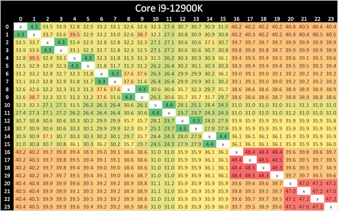
In our core-to-core latency test which showcases the physical topology of the chip, there’s a few things to note. Beginning with the P-cores, which are logically enumerated in the operating system as cores 0 to 15, we can see that latencies are about the same as what we’ve seen on Rocket Lake, although with a few nanosecond differences in the results. The latencies appear to be a bit more topologically uniform, which might indicate that Intel might have finally gotten rid of their uni-directional coherency snoop ring for a bi-directional one.
Latencies between the SMT siblings are also interesting as they decrease from 5.2ns on the Willow Cove cores to 4.3ns on the new Golden Cove cores. The actual L1 access latencies haven’t changed between the two microarchitectures, which means that Intel has improved the LOCK instruction cycle latency.
Between the Golden Cove cores and the smaller Gracemont cores we see higher latencies, as that was to be expected given their lower clock speeds and possible higher L2 overhead of the Gracemont cluster.
What’s however a bit perplexing is that the core-to-core latencies between Gracemont cores is extremely slow, and that’s quite unintuitive as one would have expected coherency between them to be isolated purely on their local L2 cluster. Instead, what seems to be happening is that even between two cores in a cluster, requests have to travel out to the L3 ring, and come back to the very same pathway. That’s quite weird, and we don’t have a good explanation as to why Intel would do this.
Cache Latencies and DDR5 vs DDR4
Next up, let’s take a look at the new cache hierarchy of Alder Lake, both from the view of the Golden Cove cores as well as the Gracemont cores, in DDR5 as well as DDR4.
Alder Lake changes up the big cores cache quite considerably. First off, the L1D remains identical – so not much to report there.
On the L2 side of things, compared to Rocket Lake’s Willow Cove cores, Alder Lake’s Golden Cove cores considerably increase the L2 cache from 512KB to 1.25MB. This does come at a 15% latency degradation for this cache, however given the 2.5x increase in size and thus higher hit rates, it’s a good compromise to make.
The Gracemont E-cores have a large 2MB L2 which is shared amongst the 4 cores in a cluster, so things do look quite differently in terms of hierarchy. Here latencies after 192KB do increase for some patterns as it exceeds the 48-page L1 TLB of the cores. Same thing happens at 8MB as the 1024-page L2 TLB is exceeded.
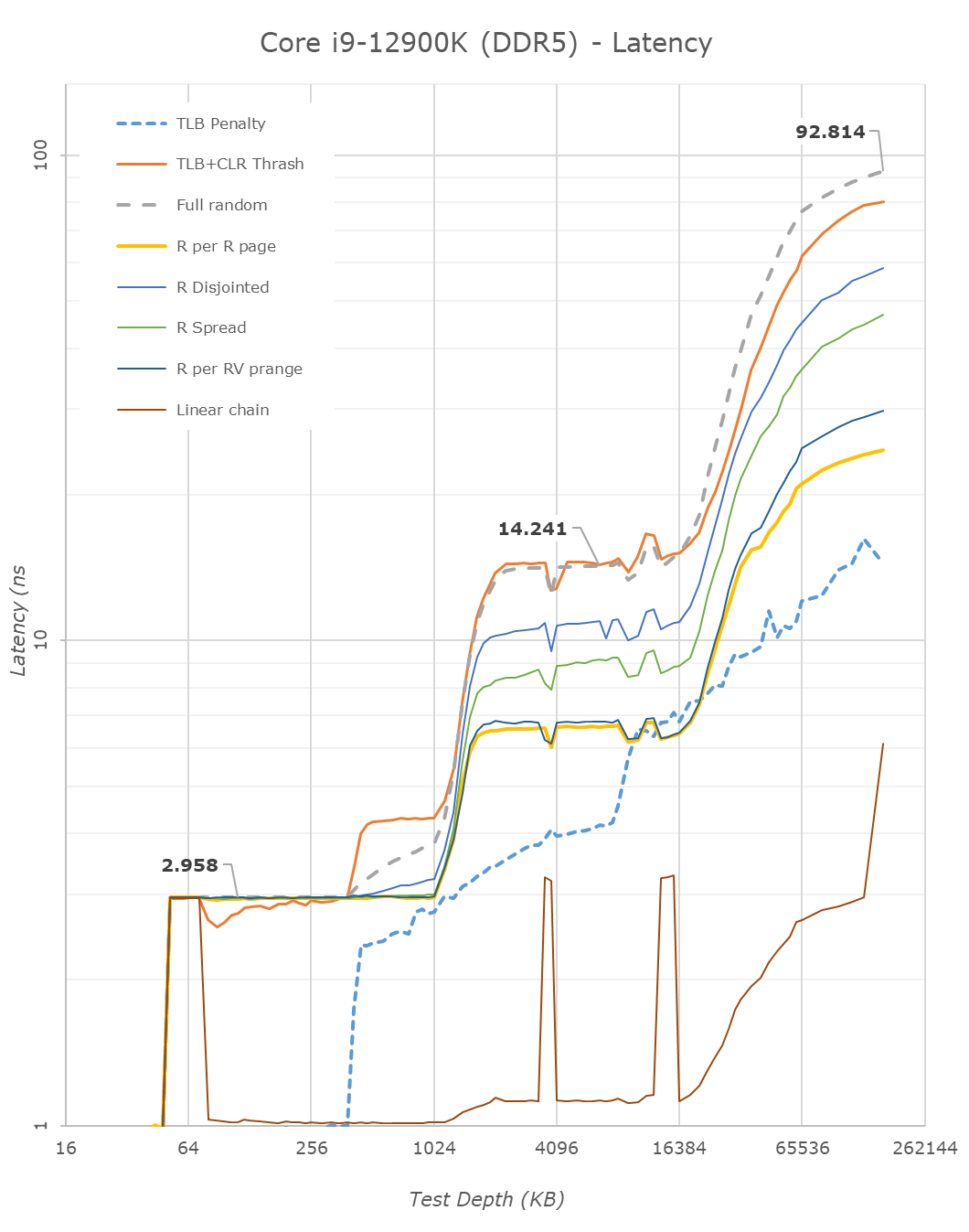
The L3 cache of the chip increases vastly from 16MB in RKL to 30MB in ADL. This increase also does come with a latency increase – at equal test depth, up from 11.59ns to 14.24ns. Intel’s ring and cache slice approach remains considerably slower than AMD’s CCX, which at a similar L3 size of 32MB comes in at 10.34ns for equivalent random-access patterns.
On the DRAM side of things, we can start off with the RKL DDR4 to ADL DDR4 results. The memory latency at 160MB goes up from 85ns to 90ns – generally expected given the larger memory subsystem of the new chip.
Shifting over from DDR4 to the DDR5 results on Alder Lake, at JEDEC speeds, comparing DDR4-3200 CL20 to DDR4-4800 CL40, the officially supported speeds of the chip, we see memory latency only go up to 92.8ns, which is actually below our expectations. In other prefetcher-friendly patterns, latency goes up by a larger 5ns, but still that’s all within reasonable figures, and means that DDR5 latency regressions we feared are overblown, and the chip is able to take advantage of the new memory type without any larger issues.
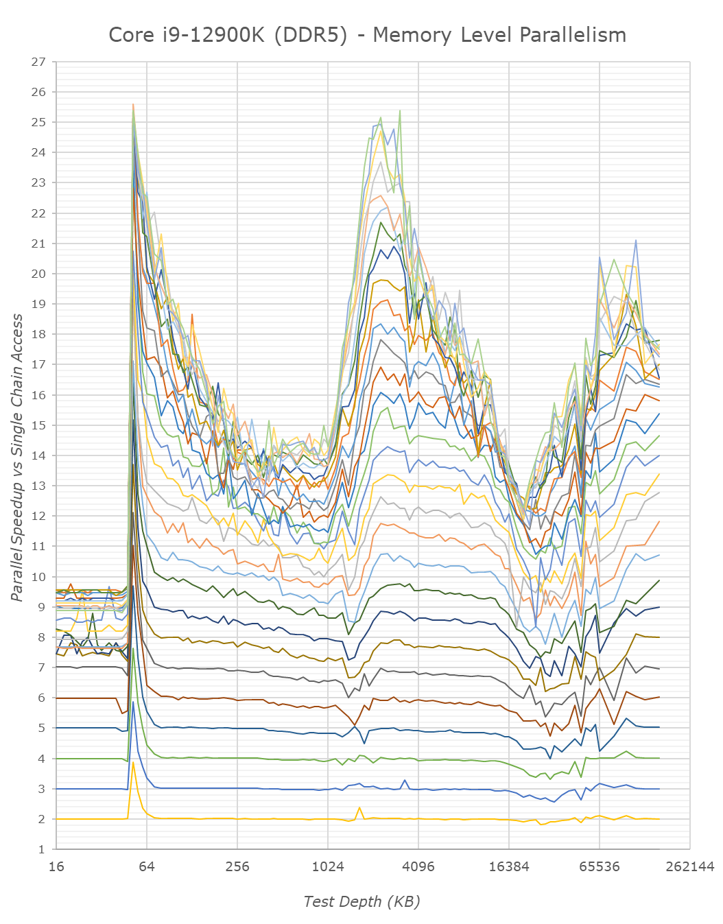
We only ever whip out our memory level parallelism test when there’s a brand-new microarchitecture which changes things quite considerably in regards to how it handles MLP. Alder Lake and its Golden Cove and Gracemont cores are such designs.
Memory level parallelism is the characteristic of a CPU being able to have multiple pending memory accesses – instead of doing things serially, out of order CPUs are able to fetch data from multiple memory locations at the same time. The definition of how many accesses this ends up as, depends on the design within the core, such as MHSR’s, but also the actual parallelism of the various caches as well as the fabric itself. Our test here compares the relative speedup of doing parallel access of random pointer chain chasing – a speedup of 2x means that the core is able to access two chains simultaneously with no degradation of per-element access times. At some point, we’ll be hitting bottlenecks of the various memory elements of the core and memory subsystem. A higher MLP speedup allows for faster execution in workloads which have data-level parallelism, and also improves the ability to hide latency in terms of performance.
Intel’s Golden Cove core is here a massive uplift in terms of its MLP capabilities. The L2 cache of the chip, because it’s so much larger, likely also has a lot more physical banks to it, likely allowing more parallel accesses.
On the L3 cache, Intel also notably mentioned that the new design is able to handle more outstanding transfers, as we immediately see this in the results of Golden Cove. Our test here only tracked up to 30 parallel accesses and we didn’t have time to check out a more extended test, but it does seem the core would be able to hit higher figures – at least until it hits TLB limits, where things slow down. The MLP capabilities here are similar, if not greater, than what AMD showcases in their Zen CPUs, something we had noted as being a strength of their microarchitecture.
MLP at deeper DRAM regions is essentially double that of Rocket Lake – at least on the DDR5 variant of Alder Lake. The DDR4 results reduce the MLP advantage, likely because the chip has to deal with only 2 memory channels rather than 4 on the DDR5 test, this allows the DDR5 variant more parallel sparse accesses to DRAM banks. Interestingly, Intel still doesn’t do as well as AMD even with DDR5 – I’m not sure where exactly the differences stem from, but it must be further down the fabric and memory controller side of things.
From the E-core Gracemont cores, the results also look good, albeit the L3 parallelism looks lower – maybe that’s a limit of the outstanding requests from the L2 cluster of the GRM cores – or maybe some interface limitation.
I think the MLP improvements of Alder Lake here are extremely massive, and represent a major jump in terms of memory performance of the design, something which undoubtedly lead to larger IPC gains for the new microarchitecture.
CPU Tests: SPEC ST Performance on P-Cores & E-Cores
SPEC2017 is a series of standardized tests used to probe the overall performance between different systems, different architectures, different microarchitectures, and setups. The code has to be compiled, and then the results can be submitted to an online database for comparison. It covers a range of integer and floating point workloads, and can be very optimized for each CPU, so it is important to check how the benchmarks are being compiled and run.
For compilers, we use LLVM both for C/C++ and Fortan tests, and for Fortran we’re using the Flang compiler. The rationale of using LLVM over GCC is better cross-platform comparisons to platforms that have only have LLVM support and future articles where we’ll investigate this aspect more. We’re not considering closed-sourced compilers such as MSVC or ICC.
clang version 10.0.0
clang version 7.0.1 (ssh://git@github.com/flang-compiler/flang-driver.git
24bd54da5c41af04838bbe7b68f830840d47fc03)
-Ofast -fomit-frame-pointer
-march=x86-64
-mtune=core-avx2
-mfma -mavx -mavx2
Our compiler flags are straightforward, with basic –Ofast and relevant ISA switches to allow for AVX2 instructions. We decided to build our SPEC binaries on AVX2, which puts a limit on Haswell as how old we can go before the testing will fall over. This also means we don’t have AVX512 binaries, primarily because in order to get the best performance, the AVX-512 intrinsic should be packed by a proper expert, as with our AVX-512 benchmark. All of the major vendors, AMD, Intel, and Arm, all support the way in which we are testing SPEC.
To note, the requirements for the SPEC licence state that any benchmark results from SPEC have to be labeled ‘estimated’ until they are verified on the SPEC website as a meaningful representation of the expected performance. This is most often done by the big companies and OEMs to showcase performance to customers, however is quite over the top for what we do as reviewers.
For Alder Lake, we start off with a comparison of the Golden Cove cores, both in DDR5 as well as DDR4 variants. We’re pitting them as direct comparison against Rocket Lake’s Cypress Cove cores, as well as AMD’s Zen3.
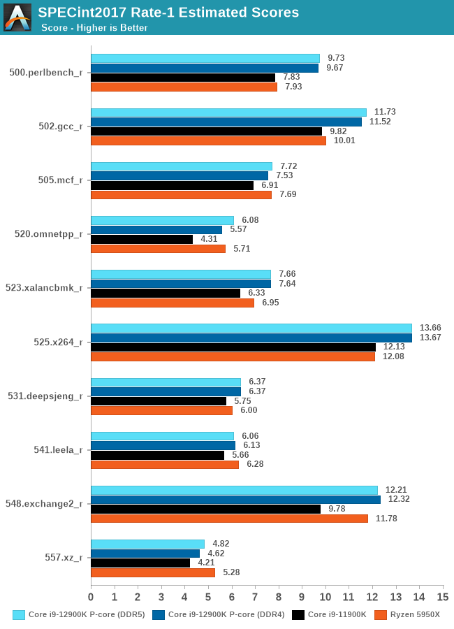
Starting off in SPECint2017, the first thing I’d say is that for single-thread workloads, it seems that DDR5 doesn’t showcase any major improvements over DDR4. The biggest increase for the Golden Cove cores are in 520.omnetpp_r at 9.2% - the workload is defined by sparse memory accessing in a parallel way, so DDR5’s doubled up channel count here is likely what’s affecting the test the most.
Comparing the DDR5 results against RKL’s WLC cores, ADL’s GLC showcases some large advantages in several workloads: 24% in perlbench, +29% in omnetpp, +21% in xalancbmk, and +26% in exchange2 – all of the workloads here are likely boosted by the new core’s larger out of order window which has grown to up to 512 instructions. Perlbench is more heavily instruction pressure biased, at least compared to other workloads in the suite, so the new 6-wide decoder also likely is a big reason we see such a large increase.
The smallest increases are in mcf, which is more pure memory latency bound, and deepsjeng and leela, the latter which is particularly branch mispredict heavy. Whilst Golden Cove improves its branch predictors, the core also had to add an additional cycle of misprediction penalty, so the relative smaller increases here make sense with that as a context.
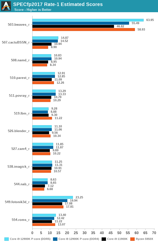
In the FP suite, the DDR5 results have a few larger outliers compared to the DDR4 set, bwaves and fotonik3d showcase +15% and +17% just due to the memory change, which is no surprise given both workloads extremely heavy memory bandwidth characteristic.
Compared to RKL, ADL showcases also some very large gains in some of the workloads, +33% in cactuBBSN, +24% in povray. The latter is a surprise to me as it should be a more execution-bound workload, so maybe the new added FADD units of the cores are coming into play here.
We’ve had not too much time to test out the Gracemont cores in isolation, but we are able to showcase some results. This set here is done on native Linux rather than WSL due to affinity issues on Windows, the results are within margin of error between the platforms, however there are a few % points outliers on the FP suite. Still, comparing the P to E-cores are in apples-to-apples conditions in these set of graphs:
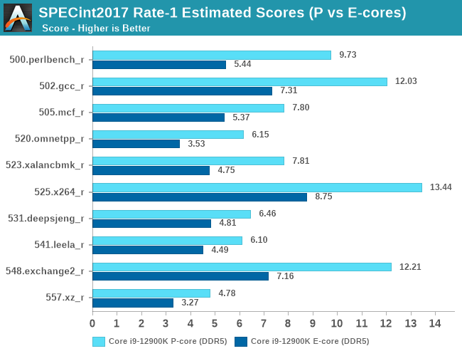
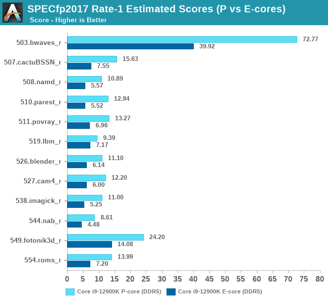
When Intel mentioned that the Gracemont E-cores of Alder Lake were matching the ST performance of the original Skylake, Intel was very much correct in that description. Unlike what we consider “little” cores in a normal big.LITTLE setup, the E-cores of Alder Lake are still quite performant.
In the aggregate scores, an E-core is roughly 54-64% of a P-core, however this percentage can go as high as 65-73%. Given the die size differences between the two microarchitectures, and the fact that in multi-threaded scenarios the P-cores would normally have to clock down anyway because of power limits, it’s pretty evident how Intel’s setup with efficiency and density cores allows for much higher performance within a given die size and power envelope.
In SPEC, in terms of package power, the P-cores averaged 25.3W in the integer suite and 29.2W in the FP suite, in contrast to respectively 10.7W and 11.5W for the E-cores, both under single-threaded scenarios. Idle package power ran in at 1.9W.
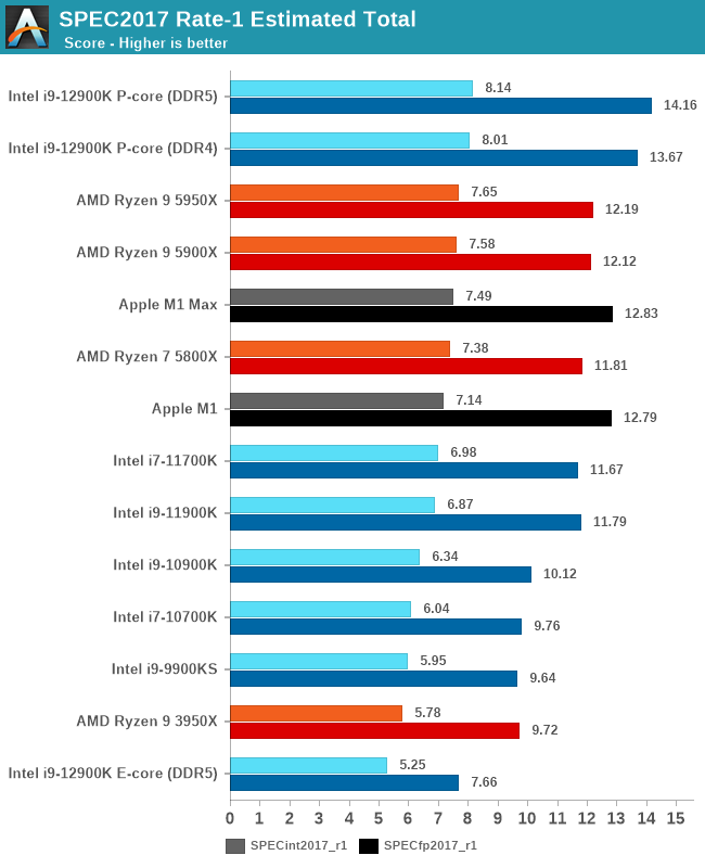
Alder Lake and the Golden Cove cores are able to reclaim the single-threaded performance crown from AMD and Apple. The increases over Rocket Lake come in at +18-20%, and Intel’s advantage over AMD is now at 6.4% and 16.1% depending on the suite, maybe closer than what Intel would have liked given V-cache variants of Zen3 are just a few months away.
Again, the E-core performance of ADL is impressive, while not extraordinary ahead in the FP suite, they can match the performance of some middle-stack Zen2 CPUs from only a couple of years ago in the integer suite.
CPU Tests: SPEC MT Performance - DDR5 Advantage
Multi-threaded performance is where things become very interesting for Alder Lake, where the chip can now combine its 8 P-cores with its 8 E-cores. As we saw, the 8 E-cores are nothing to sneeze about, but another larger consideration for MT performance is DDR5. While in the ST results we didn’t see much change in the performance of the cores, in MT scenarios when all cores are hammering the memory, having double the memory channels as well as +50% more bandwidth is going to be extremely beneficial for Alder Lake.
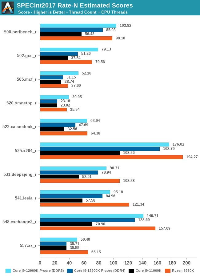
As we noted, the DDR5 vs DDR4 results showcase a very large performance gap between the two memory technologies in MT scenarios. Running a total of 24 threads, 16 for the SMT-enabled P-cores, and 8 for the E-cores, Alder Lake is able to take the performance crown in quite a lot of the workloads. There are still cases where AMD’s 16-core setup with larger cores are able to perform better, undoubtedly also partly attributed to 64MB of on-chip cache.
Compared to the 11900K, the new 12900K showcases giant leaps, especially when paired with DDR5.
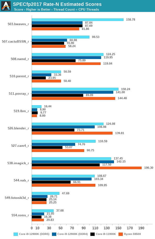
In the FP suite, the DDR5 advantage in some workloads is even larger, as the results scale beyond that of the pure theoretical +50% bandwidth improvement. What’s important for performance is not just the theoretical bandwidth, but the actual utilised bandwidth, and again, the doubled up memory channels of DDR5 here are seemingly contributing to extremely large increases, if the workload can take advantage of it.
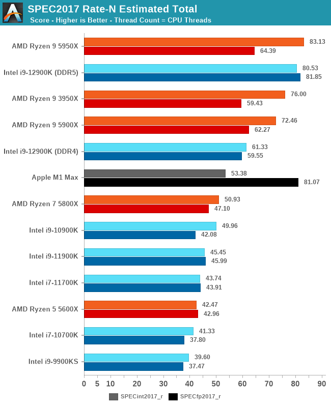
In the aggregate results, there’s very clearly two conclusions, depending on whether you use the chip with DDR5 or DDR4.
With DDR4, Alder Lake and the 12900K in particular, is able to showcase very good and solid increases in performance, thanks to the IPC gains on the Golden Cove core, but most importantly, also thanks to the extra 8 Gracemont cores, which do carry their own weight. The 12900K falls behind AMD’s 5900X with DDR4, which is fair given the pricing of the chips here are generally in line with teach other.
With DDR5, the 12900K is able to fully stretch its multi-threaded performance legs. In less memory dependent workloads, the chip battles it out with AMD’s 16-core 5950X, winning some workloads, losing some others. In more memory dependent workloads, the DDR5 advantage is extremely clear, and the 12900K is able to blow past any competition, even slightly edging out the latest Apple M1 Max, released a few weeks ago, and notable for its memory bandwidth.
CPU Tests: SPEC MT Performance - P and E-Core Scaling
Update Nov 6th:
We’ve finished our MT breakdown for the platform, investigating the various combination of cores and memory configurations for Alder Lake and the i9-12900K. We're posting the detailed scores for the DDR5 results, following up the aggregate results for DDR4 as well.
The results here solely cover the i9-12900K and various combinations of MT performance, such as 8 E-cores, 8 P-cores with 1T as well as 2T, and the full 24T 8P2T+8E scenario. The results here were done on Linux due to easier way to set affinities to the various cores, and they’re not completely comparable to the WSL results on the previous page, however should be within small margins of error for most tests.
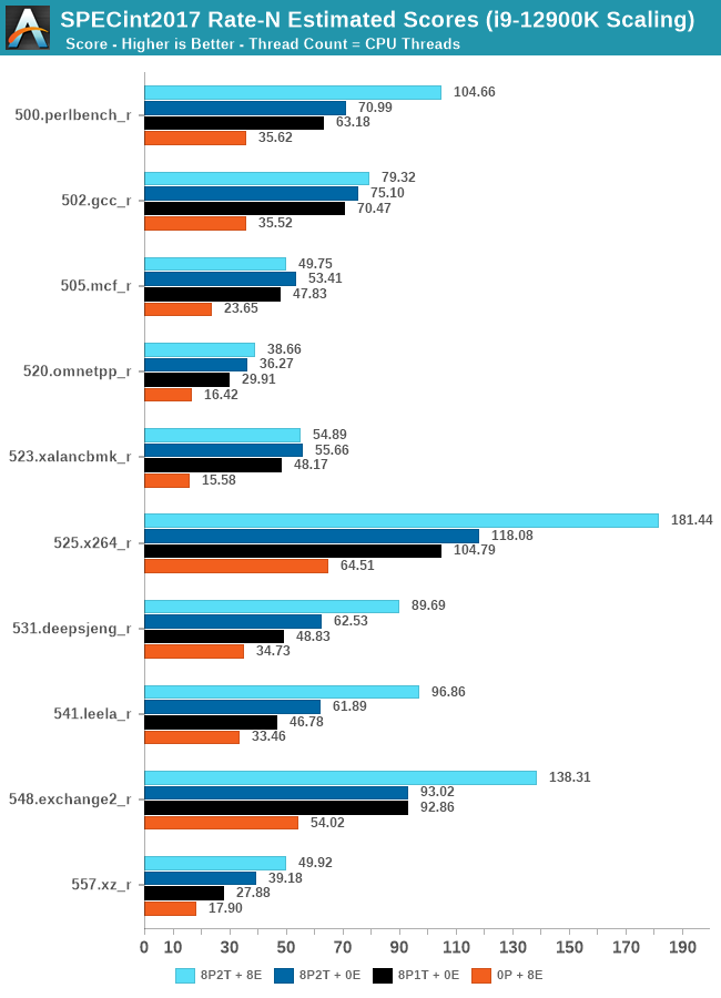
In the integer suite, the E-cores are quite powerful, reaching scores of around 50% of the 8P2T results, or more.
Many of the more core-bound workloads appear to very much enjoy just having more cores added to the suite, and these are also the workloads that have the largest gains in terms of gaining performance when we add 8 E-cores on top of the 8P2T results.
Workloads that are more cache-heavy, or rely on memory bandwidth, both shared resources on the chip, don’t scale too well at the top-end of things when adding the 8 E-cores. Most surprising to me was the 502.gcc_r result which barely saw any improvement with the added 8 E-cores.
More memory-bound workloads such as 520.omnetpp or 505.mcf are not surprising to see them not scale with the added E-cores – mcf even seeing a performance regression as the added cores mean more memory contention on the L3 and memory controllers.
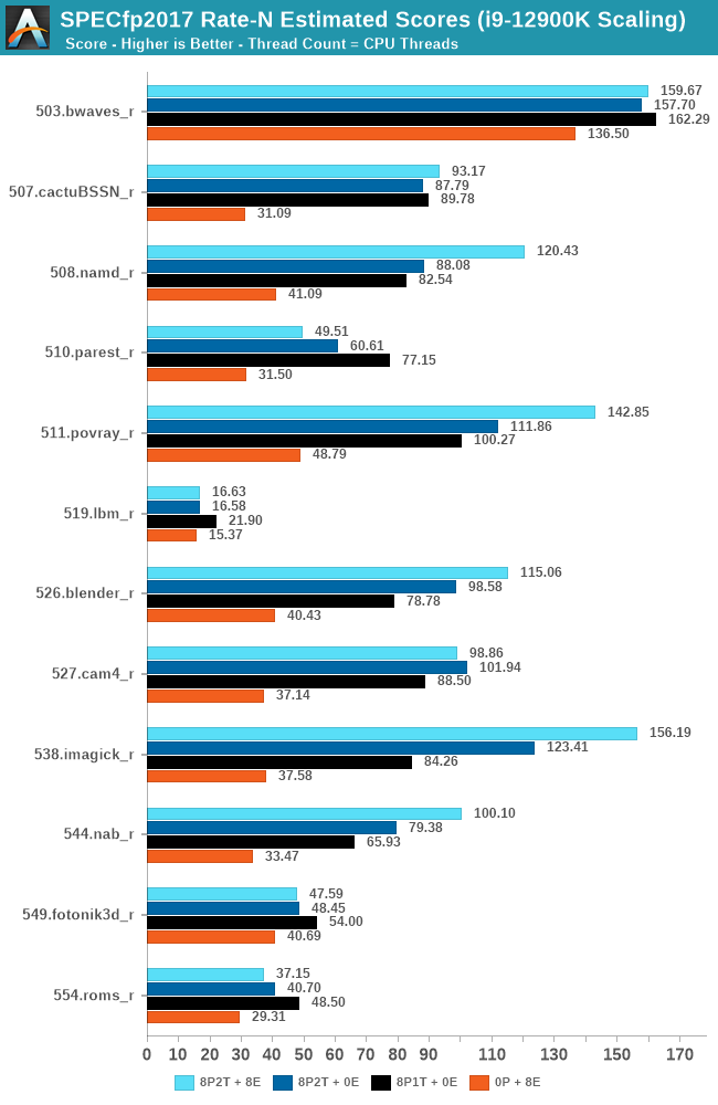
In the FP suite, the E-cores more clearly showcase a lower % of performance relative to the P-cores, and this makes sense given their design. Only few more compute-bound tests, such as 508.namd, 511.povray, or 538.imagick see larger contributions of the E-cores when they’re added in on top of the P-cores.
The FP suite also has a lot more memory-hungry workload. When it comes to DRAM bandwidth, having either E-cores or P-cores doesn’t matter much for the workload, as it’s the memory which is bottlenecked. Here, the E-cores are able to achieve extremely large performance figures compared to the P-cores. 503.bwaves and 519.lbm for example are pure DRAM bandwidth limited, and using the E-cores in MT scenarios allows for similar performance to the P-cores, however at only 35-40W package power, versus 110-125W for the P-cores result set.
Some of these workloads also see regressions in performance when adding in more cores or threads, as it just means more memory traffic contention on the chip, such as seen in the 8P2T+8E, 8P2T regressions over the 8P1T results.
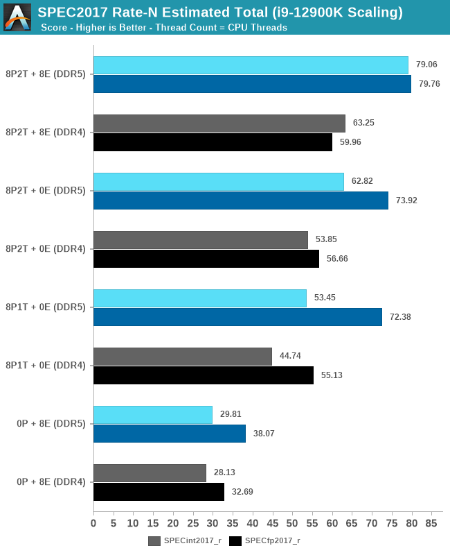
What’s most interesting here is the scaling of performance and the attribution between the P-cores and the E-cores. Focusing on the DDR5 set, the 8 E-cores are able to provide around 52-55% of the performance of 8 P-cores without SMT, and 47-51% of the P-cores with SMT. At first glance this could be argued that the 8P+8E setup can be somewhat similar to a 12P setup in MT performance, however the combined performance of both clusters only raises the MT scores by respectively 25% in the integer suite, and 5% in the FP suite, as we are hitting near package power limits with just 8P2T, and there’s diminishing returns on performance given the shared L3. What the E-cores do seem to allow the system is to allows to reduce every-day average power usage and increase the efficiency of the socket, as less P-cores need to be active at any one time.
CPU Benchmark Performance: E-Core
In this batch of testing, we're focusing primarily on the E-cores. Intel claimed that the performance was around the level of its Skylake generation of processors (6th Gen to 10th Gen, depending which slide you read), and we had to put that to the test. In this instance, we're comparing to the flagship Skylake processor, the Core i7-6700K, which offered 4C/8T at 91 W. We also did a number of multi-threaded tests to see where the E-cores would line up.
In order to enable E-core only operation, we used affinity masks.
Single Threaded


In these few tests, we can see that the E-core is almost there at 4.2 GHz Skylake. Moving down to 3.9 GHz, perhaps something like the i7-6700, would put it on par.
Multi-Thread Tests


Having a full eight E-cores compared to Skylake's 4C/8T arrangement helps in a lot of scenarios that are compute limited. When we move to more memory limited environments, or with cross-talk, then the E-cores are a bit more limited due to the cache structure and the long core-to-core latencies. Even with DDR5 in tow, the E-cores can be marginal to the Skylake, for example in WinRAR which tends to benefit from cache and memory bandwidth.
CPU Performance: Windows 11 vs Windows 10
There are going to be a lot of Windows 11 vs Windows 10 testing over the next few months, based on different CPUs, chipsets, configurations, and even situations where CPUs are replaced and drivers need to be reinstalled to get full performance. Windows 11 is still young, and most of our tests worked (WSL did not, will need to find out why). In this instance both OS installs were fresh and default with all updates and updated drivers. We haven't had time to run our gaming tests, those should come soon.


Windows 11 has a small effect on some of our Multi-Threaded tests, such as y-cruncher, Speedometer, and AES, but for the most part it's quite minimal.
CPU Benchmark Performance: DDR5 vs DDR4
Traditionally we test our memory settings at JEDEC specifications. JEDEC is the standards body that determines the requirements for each memory standard. In this case, the Core i9 supports the following aligning with those standards:
- DDR4-3200 CL22
- DDR5-4800B CL40*
There's an * next to the DDR5 for a couple of reasons. First, when asked, Intel stated that 4800A (CL34) was the official support, however since the technical documents have now been released, we've discovered that it is 4800B (CL40). Secondly, 4800B CL40 technically only applies to 1 module per 64-bit channel on the motherboard, and only when the motherboard has two 64-bit slots to begin with. We covered Intel's memory support variants in a previous article, and in this instance, we're using DDR5-4800B memory in our testing.


As explained in our SPEC section, DDR5 memory not only brings bandwidth improvements but also the increased number of channels (4x32-bit vs 2x64-bit) means that the memory can be better utilized as threads pile on the memory requests. So while we don't see much improvement in single threaded workloads, there are a number of multi-threaded workloads that would love the increased performance.
Gaming Performance: DDR5 vs DDR4
All of our game testing results, including other resolutions, can be found in our benchmark database: www.anandtech.com/bench. All gaming tests were with an RTX 2080 Ti.
1080p Max


4K Low
CPU Benchmark Performance: Intel vs AMD
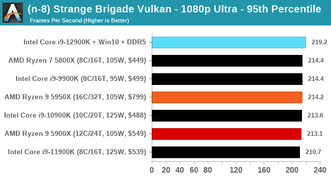
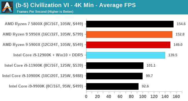
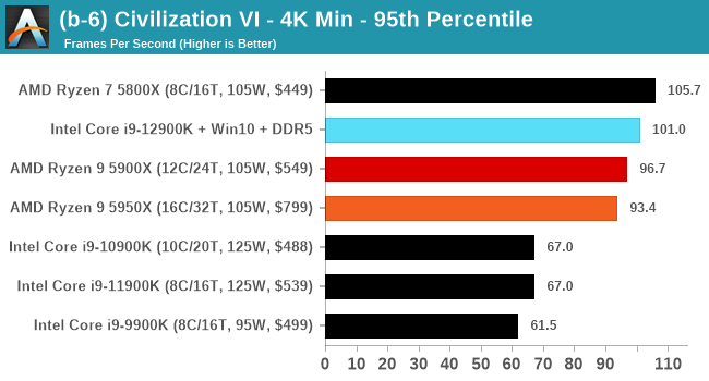
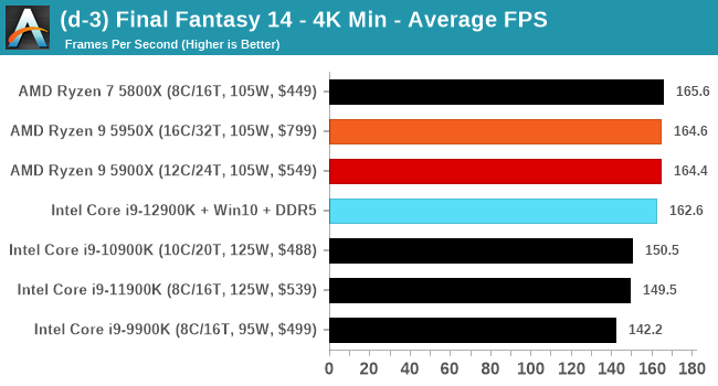
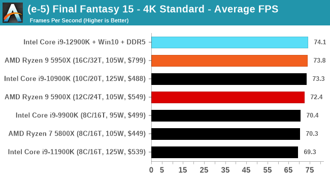
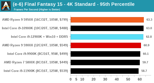
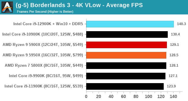
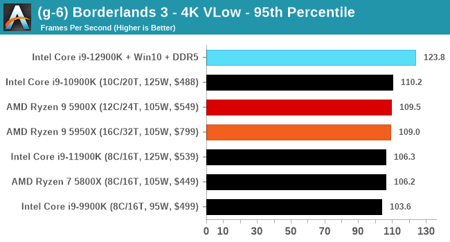
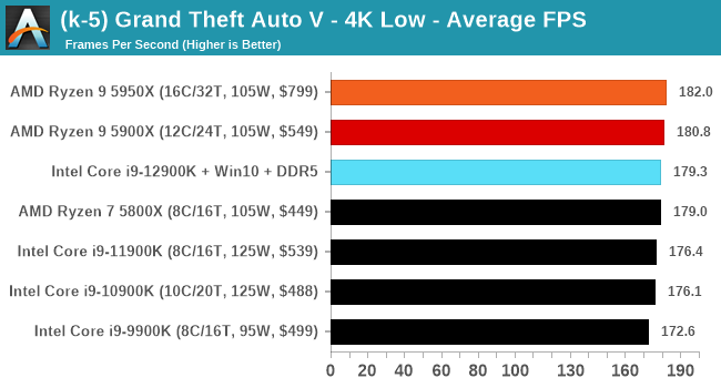
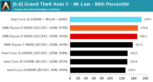
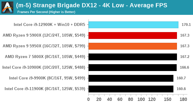
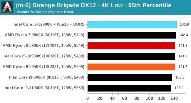
Here are the graphs you've probably be wanting to see. Here we've listed Intel's last few flagships, along with AMD's Zen 3 offerings. In no particular order, here is the CPU performance.
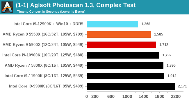
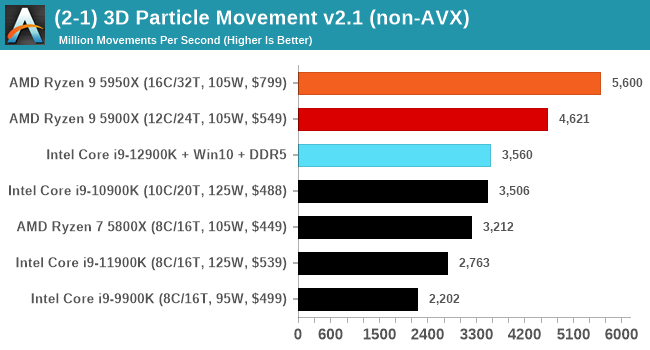

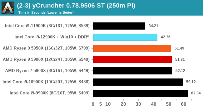
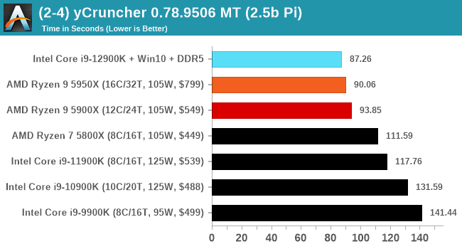
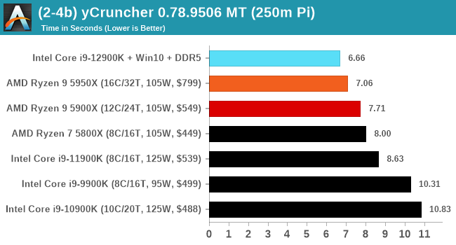
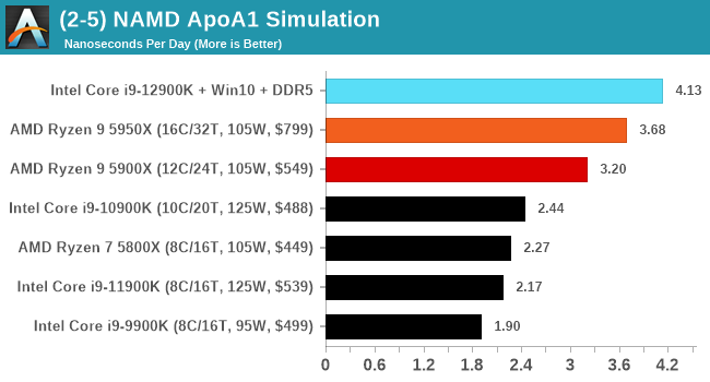
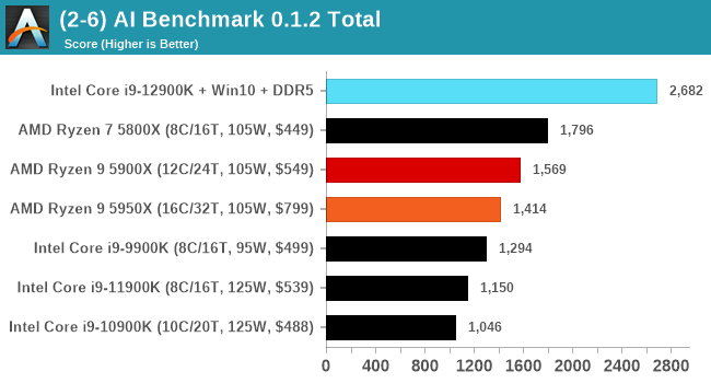
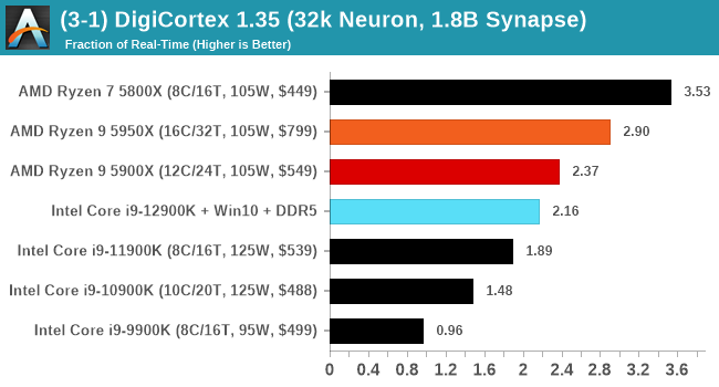
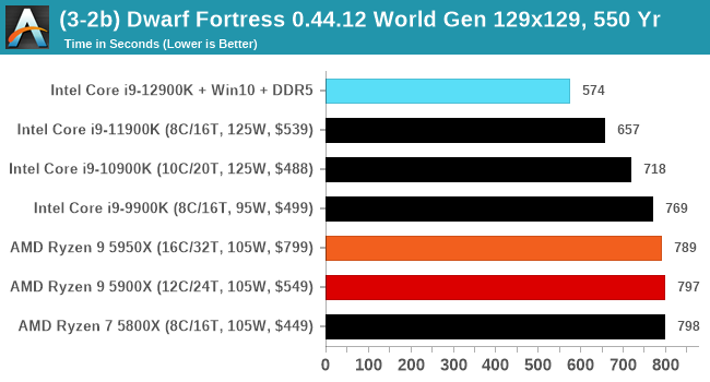
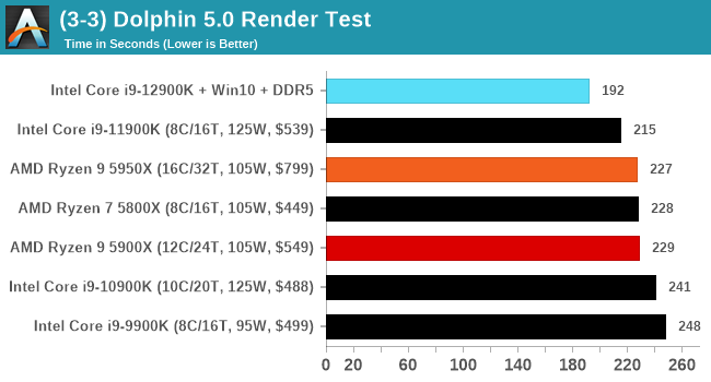
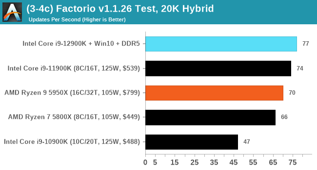
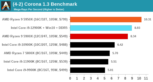
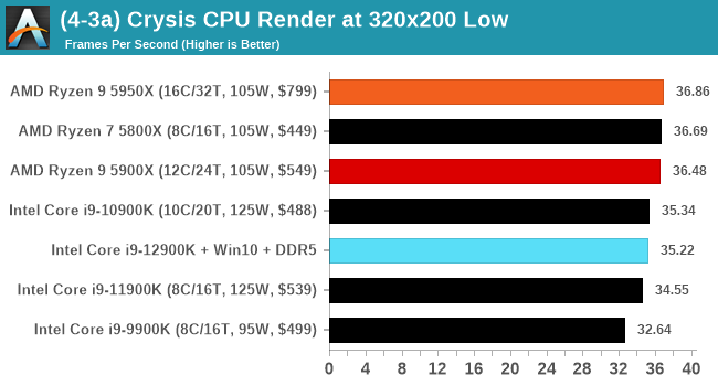
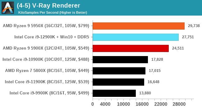
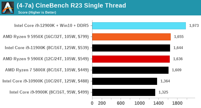
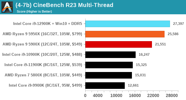
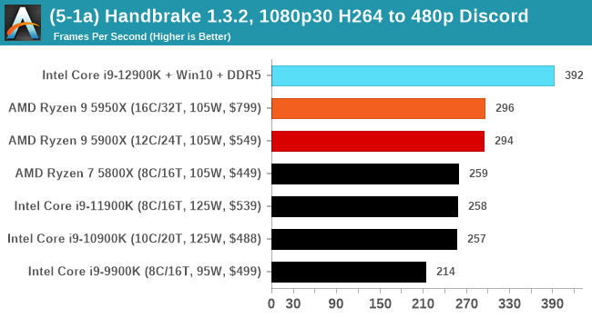
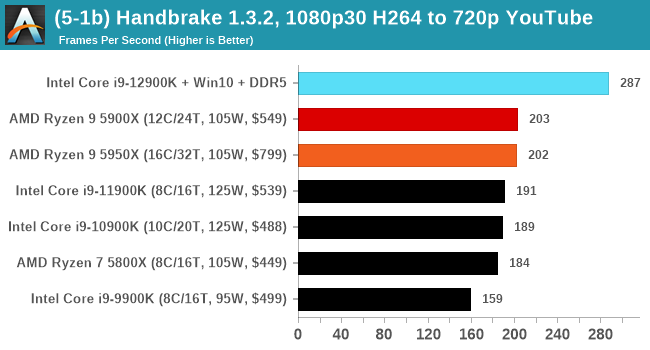
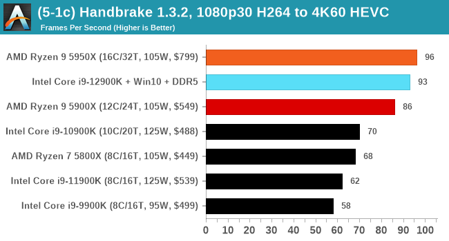
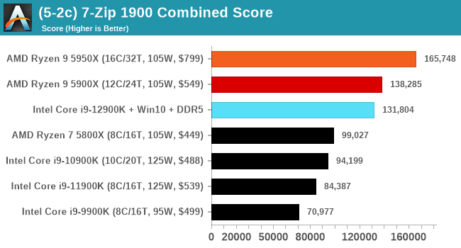
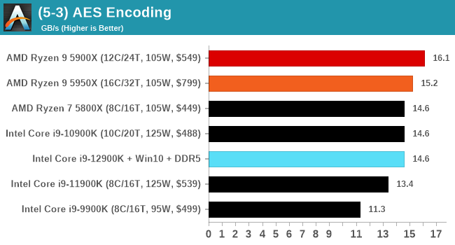
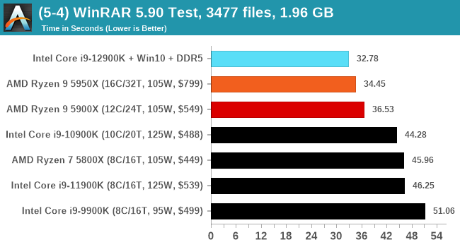
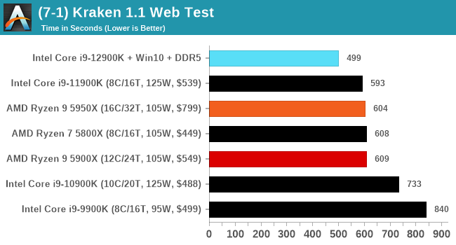
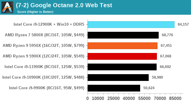
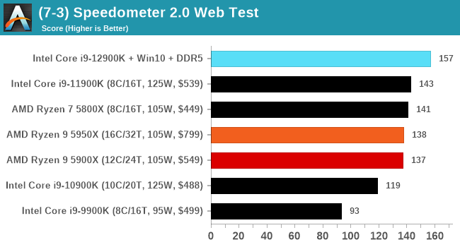
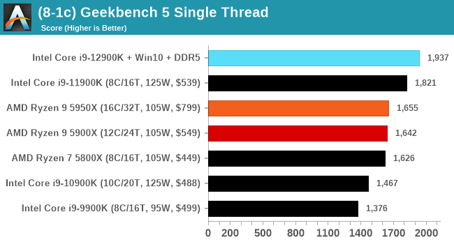
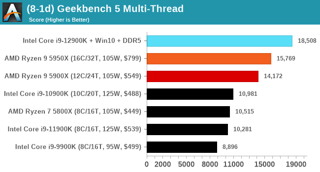
It's hard to miss a lot of blue bars at the top of these charts. ST performance usually reigns supreme, and it shines though. Intel does take a few other wins here in multi-threaded as well, and users will point to CineBench. CB loves lightweight threads and cores, and with the combined improvements in the out-of-order window in both cores as well as memory access improvements into the L2 caches.
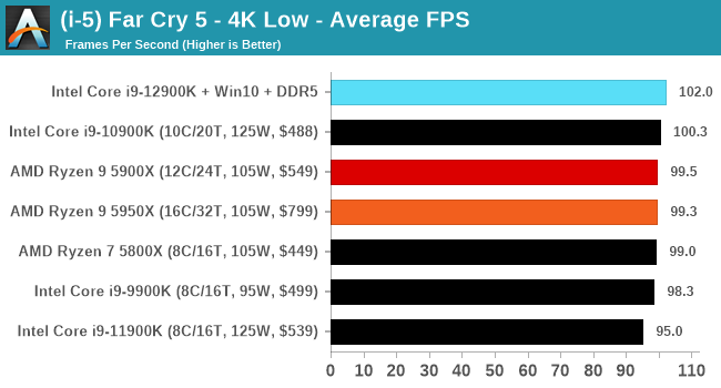
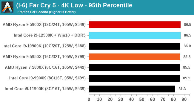
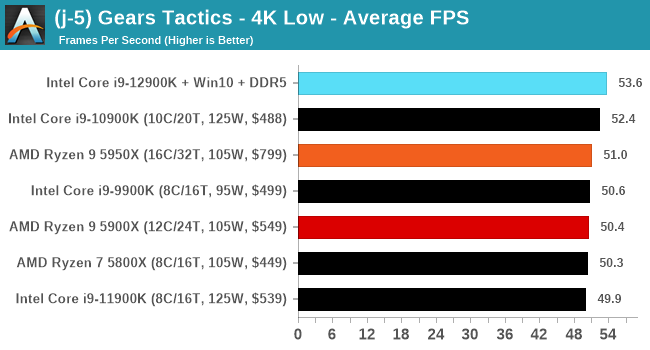
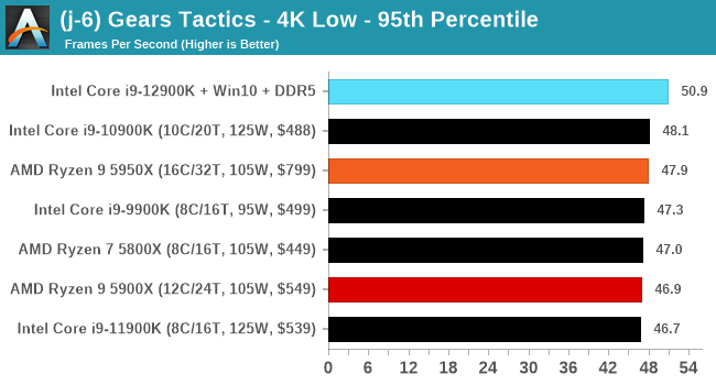
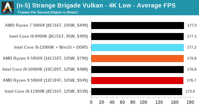
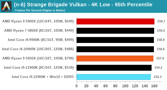
Gaming Performance: Intel vs AMD
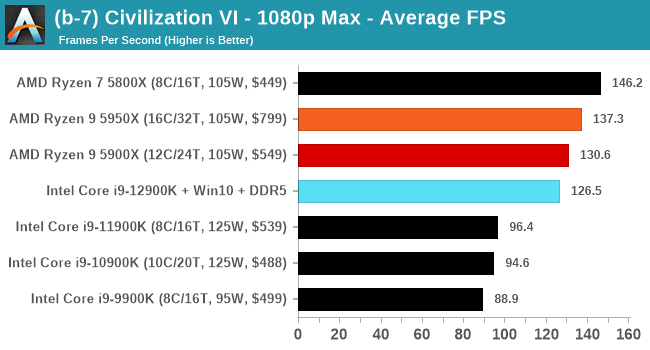
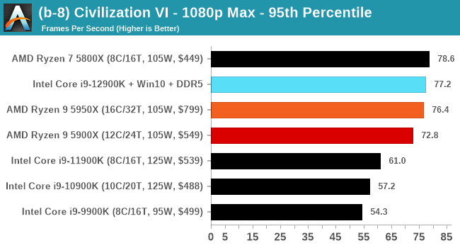
All of our game testing results, including other resolutions, can be found in our benchmark database: www.anandtech.com/bench. All gaming tests were with an RTX 2080 Ti.
1080p Max
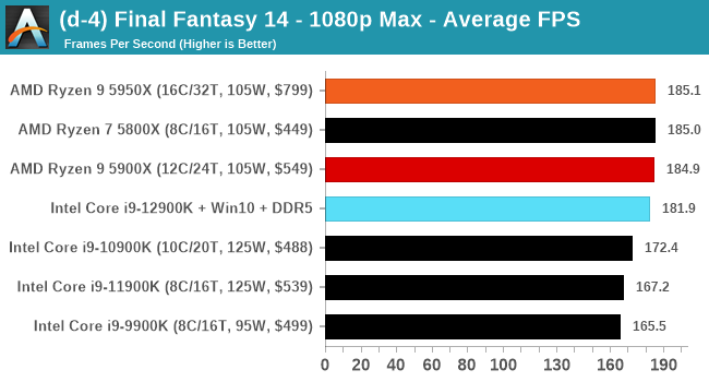
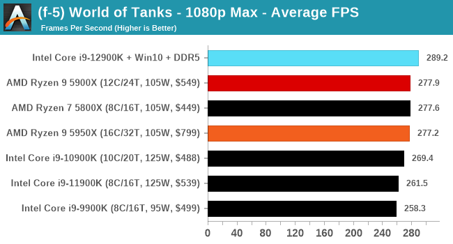
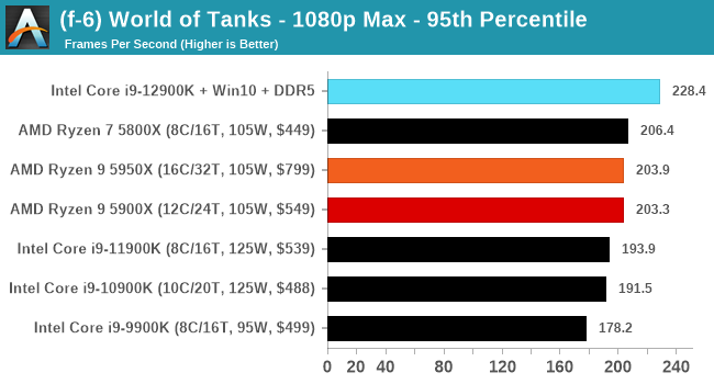
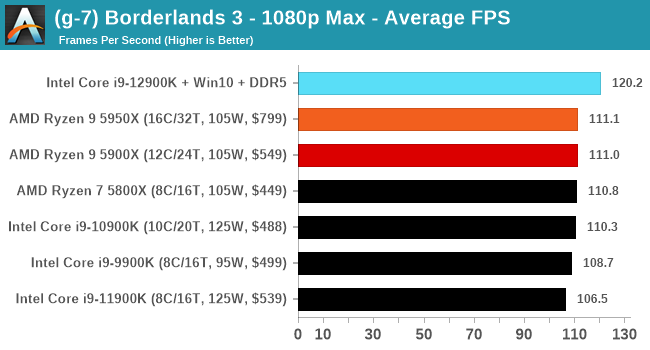
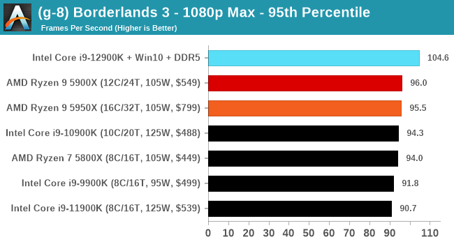
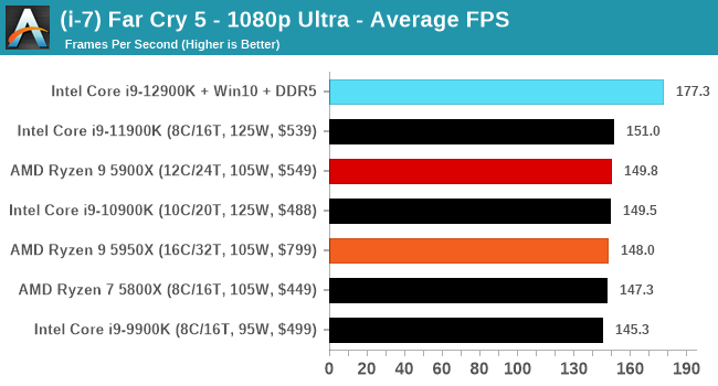
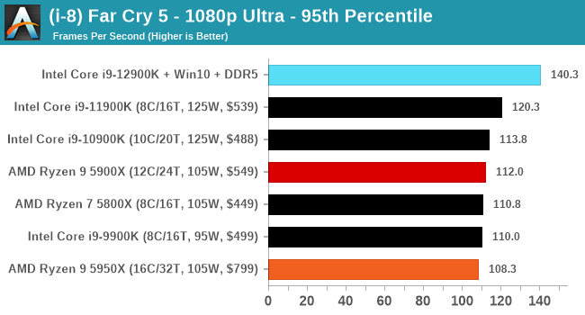
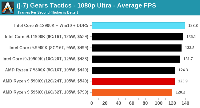
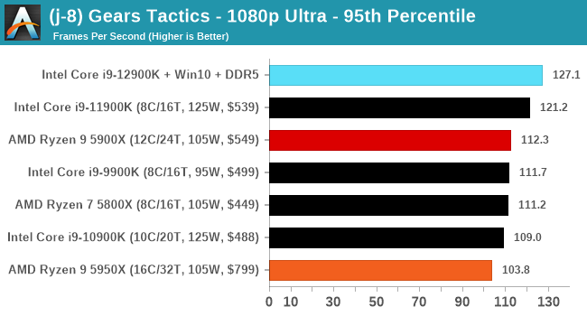
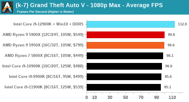
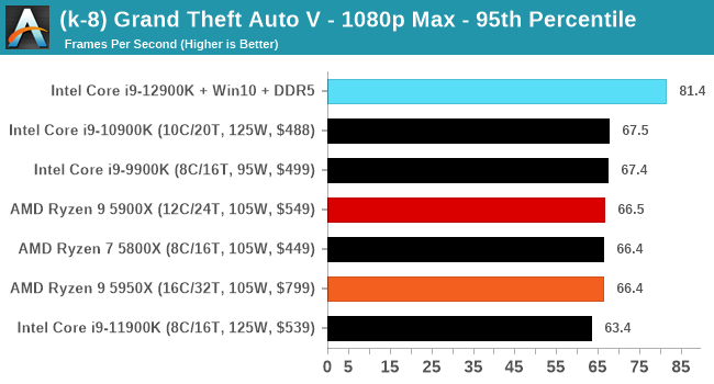
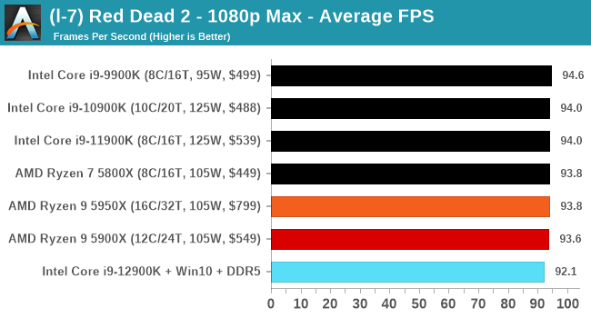
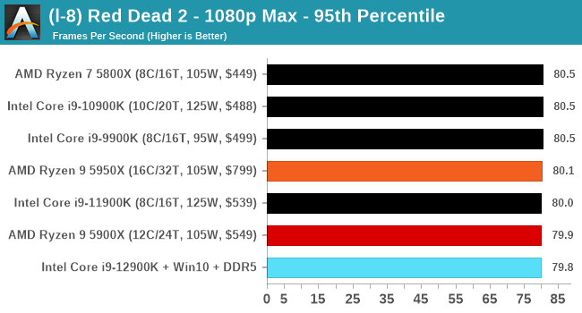
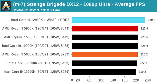
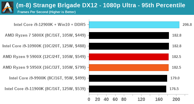
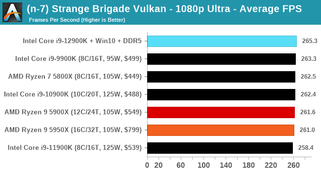
4K Low
Conclusion: Variables Maketh the CPU
Suffice to say, Intel’s new 12th Generation Core family has added more variables to the mix than a traditional processor launch. The combination of different types of core, coming at a time where a new operating system has just been launched, but also at the inflection point of a new type of memory. Let’s break down some of the differences we’ve observed in our testing.
When we compare Windows 10 to Windows 11, purely on throughput benchmarks, we don’t find much difference. There are a few spots where Windows 11 has a slight advantage in multi-threaded workloads, but this comes down to how new threads are spawned between the performance cores and the efficiency cores. Intel stated that the performance between the two, at least for CPU workloads, should be within a few percentage points, stating that Windows 11 should have lower run-to-run variance. We can corroborate this in our testing. Windows 10 also had some scheduling issues with low priority threads, which we expect to be ironed out with updates.
Comparing the new DDR5 to the old DDR4 is a different story, as the new memory standard offers a substantial uplift when it comes to memory bandwidth. As we saw recently with the M1 Max review, sometimes memory bandwidth can be a limiting factor. In our testing, DDR5 had a minor lead in single threaded tests but in a lot of multithreaded tests, the lead was significant. For real world, we had examples of +14% in Agisoft, +10% in NAMD, +8% in V-Ray, +10% in Handbrake, and +20% in WinRAR. In SPEC2017, we saw a couple of single threaded workloads get +15% improvements over DDR5, but in multi-threaded this was up to +40% on average, or more than 40% in specific tests. This also comes down to the doubled memory channels (4x32-bit vs 2x64-bit) which can be better utilized on top of the bandwidth increases.
Now comparing the P-core to the E-core, and it’s a story of how the E-core individually can perform on par with a Skylake core. Having eight extra Skylake-class cores is nothing to be sniffed at. In a lot of tests the E-core is half the performance of the P-core, but the P-core is itself is now the market leader in performance. The Golden Cove core inside Alder Lake has reclaimed the single-threaded performance crown with an uplift in SPEC of 18-20%, which is in line with Intel’s 19% claim. This puts it ahead of Apple’s M1 Max or 6% (int) and 16% (fp) ahead of AMD’s Zen 3 core.
The Core i9-12900K
Combining fast P-cores, Skylake-class E-cores, and DDR5 into one package means that Intel has certainly jumped from behind the competition to in front of it, or at least in the mix. When you have your operating system set up just right, and no issues with schedulers, it outperforms AMD’s offering when single core performance matters, and in multi-threaded workloads, it does tend to sit somewhere between a 5900X and a 5950X.

It’s important to note that in some tests, the Core i9-12900K does win outright. It’s at this point we should consider how much is core related vs standards related: DDR5 has produced somewhat of an uplift, and the competition is expected to claw some of that back when they introduce it, but those products are expected more towards the latter half of 2022. For users with those specific workloads today, and willing to pay the DDR5 early adopter tax, Alder Lake can provide performance uplifts right now.

Power is an interesting topic, and although our peak power numbers when all cores were loaded were above the 241W Turbo power on the box, in real world workloads it didn’t tend to go that high. The P-cores alone on the chip matched the power consumption of Intel’s 11th Generation in AVX2 workloads, but adding in the E-cores does put it over the previous generation. I’m not entirely sure what that says about Intel’s 7 manufacturing process compared to the 10SF used before. A lot of the performance gains here appear to come from IPC and DDR5, and that doesn’t seem to have come with performance per watt gains on the P-cores. It means that Intel is still losing on power efficiency at load compared to the competition.

I have to say a side word about AVX-512 support, because we found it. If you’re prepared to disable the E-cores, and use specific motherboards, it works. After Intel spent time saying it was fused off, we dug into the story and found it still works for those that need it. It’s going to be interesting to hear how this feature will be discussed by Intel in future.
Overall though, it’s no denying that Intel is now in the thick of it, or if I were to argue, the market leader. The nuances of the hybrid architecture are still nascent, so it will take time to discover where benefits will come, especially when we get to the laptop variants of Alder Lake. At a retail price of around $650, the Core i9-12900K ends up being competitive between the two Ryzen 9 processors, each with their good points. The only serious downside for Intel though is cost of switching to DDR5, and users learning Windows 11. That’s not necessarily on Intel, but it’s a few more hoops than we regularly jump through.

