The Crucial MX500 500GB SSD Review: A Second Look
by Billy Tallis on February 2, 2018 9:30 AM ESTAnandTech Storage Bench - The Destroyer
The Destroyer is an extremely long test replicating the access patterns of very IO-intensive desktop usage. A detailed breakdown can be found in this article. Like real-world usage, the drives do get the occasional break that allows for some background garbage collection and flushing caches, but those idle times are limited to 25ms so that it doesn't take all week to run the test. These AnandTech Storage Bench (ATSB) tests do not involve running the actual applications that generated the workloads, so the scores are relatively insensitive to changes in CPU performance and RAM from our new testbed, but the jump to a newer version of Windows and the newer storage drivers can have an impact.
We quantify performance on this test by reporting the drive's average data throughput, the average latency of the I/O operations, and the total energy used by the drive over the course of the test.
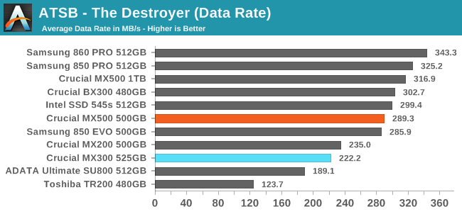
The Crucial MX500 500GB delivers a slightly slower average data rate on The Destroyer than the Intel 545s or the Crucial BX300, but it is still substantially faster than previous MX series drives. The MLC drives are on top, but the Samsung 860 PRO's lead is less than 15%. This time last year, the top MLC drive held a 46% advantage over Crucial's TLC-based MX300.
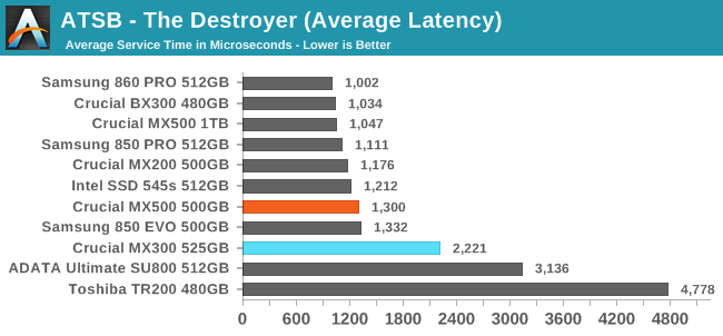
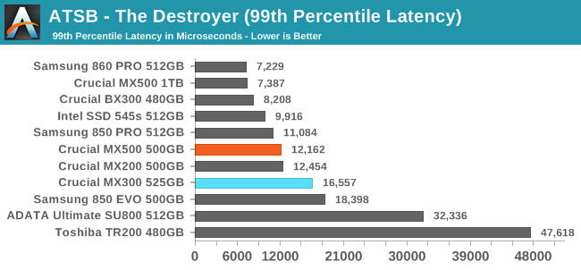
The average and 99th percentile latency scores of the Crucial MX500 500GB are good but still lag behind the MLC based drives and the Intel 545s. The MX500's average latency is essentially tied with the Samsung 850 EVO, and its 99th percentile latency is clearly better.
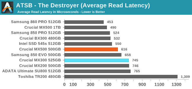
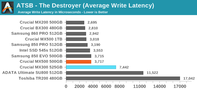
The average read and write latency scores for the Crucial MX500 are both slower than the Intel 545s, but are at least as fast as any other TLC based drive, including the Samsung 850 EVO.
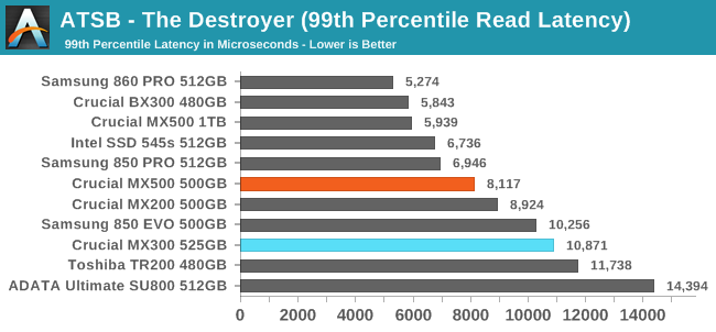
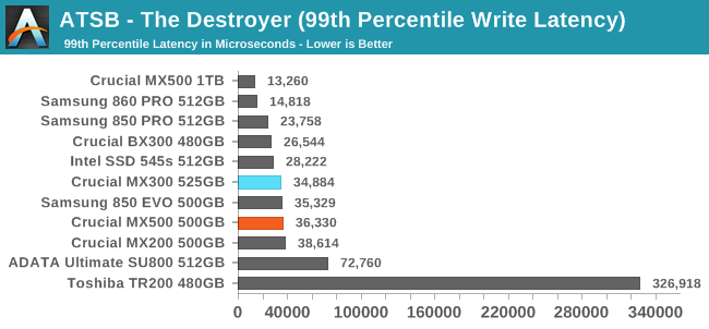
The 99th percentile read latency of the MX500 is much better than the MX300, but the 99th percentile write latency score has barely improved. In both cases, that leaves the MX500 trailing the Intel 545s but ahead of the Samsung 850 EVO.
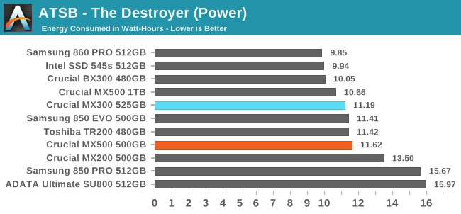
The power consumption of the Crucial MX500 on The Destroyer is slightly higher than the MX300, and is clearly worse than the Intel 545s or the Crucial BX300. The regression relative to the MX300 isn't serious enough to worry mobile users, but it probably means the MX500 will end up being the least power-efficient mainstream SATA SSD of its generation, once we've tested the 860 EVO.


25 Comments
View All Comments
PeachNCream - Friday, February 2, 2018 - link
"..the per-die capacity of the MX500's 64-layer 3D TLC is actually lower than that of the 32L 3D TLC.."Why is that the case? Shouldn't doubling the number of layers lead to greater capacity and does this mean that there are more ICs per GB in the newer MX500? I'm super confused.
jtd871 - Friday, February 2, 2018 - link
"The Crucial MX500 uses Micron's 256Gb 64L 3D TLC part and consequently returns to the standard drive capacities and overprovisioning ratios, instead of the unusual configurations caused by the 384Gb die capacity in the MX300's 32L 3D TLC. The slightly lower usable capacities of the MX500 than the MX300 means the new drives have slightly higher prices on a per-GB basis, but the MSRPs are still very competitive against current street prices for the competition."So the new chips have more layers per package, but less overall capacity. I'll guess the 384Gb die hamstrung performance on relatively smaller-capacity drives by offering fewer memory channels for the processor to work with simultaneously. Plus, I'll guess that it was a bit of an oddball size for the algorithms to deal with.
FunBunny2 - Friday, February 2, 2018 - link
large node?more area dedicated to control functions?
Billy Tallis - Friday, February 2, 2018 - link
For the 32L node, IMFT was more or less prioritizing MLC use cases by making a 256Gb MLC die that could be used as a 384Gb TLC part. For the 64L node, TLC is the priority and they're making both 256Gb TLC and 512Gb TLC parts. The latter should be cheaper per GB when it is available, but would be a worse choice for small consumer drives. The 256Gb die is really tiny, which makes it more appealing to the mobile market than a lot of previous IMFT parts.FunBunny2 - Saturday, February 3, 2018 - link
"making a 256Gb MLC die that could be used as a 384Gb TLC part."so... does this mean that NAND is all the same, and it's the controller that decides among S/M/T?? or is it the case that S can be coerced to M, and M to T, but not the other way round? is there a tute, here or elsewhere, that tells us the nittygritty about why titular NAND can/can't be used at other densities?
FunBunny2 - Saturday, February 3, 2018 - link
well, I did find one, but from 2012 (and AT: https://www.anandtech.com/show/5067/understanding-... )"This array can be turned into either SLC, MLC, or TLC. The actual array and transistors are equivalent in all three flash types; there is no physical difference. "
some/many folks have been claiming that TLC, in particular, is physically different from SLC. is that now true?
Kristian Vättö - Sunday, February 4, 2018 - link
In terms of memory cell design, SLC, MLC and TLC can be the same, but the peripheral circuit design isn't (min # of latches = # of bits per cell). More bits per cell designs are also likely to have more spare/ECC bytes per page.In layman terms, TLC and MLC can be run as pseudo-SLC by only programming the lower page, but it's impossible to run e.g. MLC as TLC. But pseudo-SLC isn't the same thing as native SLC.
Spatty - Wednesday, February 14, 2018 - link
SLC/MLC chips are physically the same chips during the fab process. Maybe some Implant changes but die layout is the same. In Probe, circuits are blown to make them SLC or MLC.The referenced quote in this thread, is that a due to the usage of die vs chip/package. The chips in the images can have multiple die in one single chip/package and thus the 'density' of the chip/package changes. More layers still means more bits/mm^2.
PeachNCream - Monday, February 5, 2018 - link
Thanks Billy! It makes more sense now.colonelclaw - Friday, February 2, 2018 - link
I'm wondering, would it be worth adding a PS4 Pro/'BoneX benchmark to SATA SSD reviews? The 1TB is fast becoming a worthwhile, if luxurious, upgrade for the top consoles. It may be slightly unaffordable now, but possibly not for long?