Assessing Cavium's ThunderX2: The Arm Server Dream Realized At Last
by Johan De Gelas on May 23, 2018 9:00 AM EST- Posted in
- CPUs
- Arm
- Enterprise
- SoCs
- Enterprise CPUs
- ARMv8
- Cavium
- ThunderX
- ThunderX2
ThunderX: From Small & Simple to Wide & Complex
As a brief recap, the original ThunderX was an improved version of the Octeon III: a dual-issue in-order CPU core with two short pipelines.
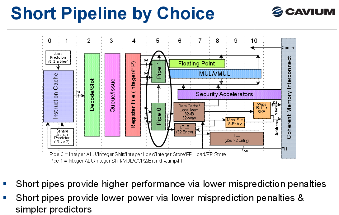
The advantage of the original ThunderX design is that such a simple core can be very energy efficient, especially for "low ILP" (instruction level parallelism) workloads such as web servers and most database servers. Of course, such a short pipeline limits the clockspeed, and such a simple in-order design offers low single threaded performance in medium and high ILP workloads, whereas more advanced out-of-order processors can extract significant parallelism.
Cavium's "New" Core: Vulcan
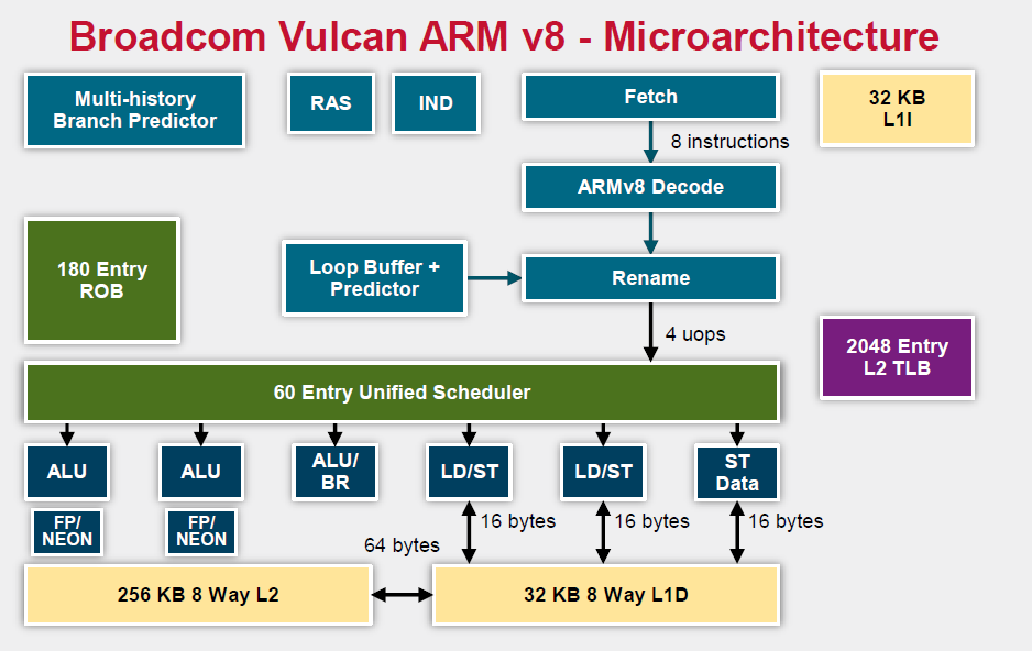
Relative to the original ThunderX, the Vulcan core of the ThunderX2 is an entirely different beast. Announced in 2014 by Broadcom, it is a relatively wide core that runs 4 simultaneous threads (SMT4). As a result, the wide back end should be quite busy even when running low-ILP server workloads.
To make sure that all 4 SMT threads can be sustained, the ThunderX2 front-end can fetch up to 64 bytes from the 8-way set associative 32 KB instruction cache, which is outfitted with a simple next line prefetcher. However, fetching 8 instructions is only possible if there is no taken branch inside those 64 bytes. In that case, the fetch breaks off at the taken branch.
That means that in branch intensive code (databases, AI...) the fetcher will get +/- 5 instructions per clock cycle on average, as one out of 5 instructions is a branch. The fetched instructions are then sent to a smoothing buffer – a buffer where the fetched instructions are held for decoding.
The decoder will then work on a bundle of 4 instructions. Between the decoder and the rename phase each thread has "skid buffer" which consists of 8 bundles. So between the 4 threads up to 32 bundles (128 instructions) can be skid buffered at any one time..
Those 4 instructions – a bundle – travel together through the pipeline until they reach the unified issue queue of the scheduler. Just like Intel has implemented in Nehalem, there is also a loop buffer and predictor, which Intel used to call a "Loop Stream Detector". This loop buffer avoids branch mispredictions and contains decoded µops, which "shortens" the pipeline and reduces the amount of power spent on decoding.
Overall, up to 6 instructions can be executed at the same time. This is divided into 2 ALU/FP/NEON slots, 1 ALU/branch slot, 2 load/store slots (16 bytes), and 1 pure store slot that sends 16 bytes to the D-cache. There is a small (Cavium would not disclose how small) L1 TLB for zero latency translation from Virtual to physical addresses. There is no hardware prefetcher for the L1 D-cache, but the L2 cache has a rather complex hardware prefetcher which is able to recognize patterns (besides being able to stride or fetching the next line).
This is enough to feed the back-end, which can sustain 4 instructions per cycle from 4 different threads.
Micro Architecture Differences
Ultimately Cavium has only published a limited amount of information on the ThunderX2 cores, so there are some limits to our knowledge. But we've gone ahead and summarized some of the key specifications of the different CPU architectures below.
| Feature | Cavium ThunderX2 |
Qualcomm Centriq "Falkor" |
Intel "Skylake"-SP |
AMD EPYC "Zen" |
| L1-I cache Associativity |
32 KB 8-way |
64KB 8-way (+ 24 KB L0) |
32 KB 8-way |
64KB 4-way |
| L1-D cache Associativity |
32 KB 8-way |
32 KB 8-way* |
32 KB 8-way |
32 KB 8-way |
| Load Bandwith | 2x 16B | 2x 16B | 2x 32B | 2x 16B |
| L2-cache | 256 KB 8-way |
256 KB 8-way |
1 MB 16-way |
512 KB 8-way |
| Fetch Width | 8 instructions | 4 instructions | 16 bytes (+/- 4-5 x86) | 32 bytes (+/- 6-8 x86) |
| Issue Queue | 60 | 76 | 97 unified | 6x14 |
| Sustainable Instructions/cycle | 4 | 4 | 5-6 | 4-5 |
| Instructions in Flight | 180 (ROB) | 128 | 224 (ROB) | 192 |
| Int. Pipeline Length |
? |
15 stages | 19 stages 14 stage from µop cache |
19 stages? |
| TLB Instructions TLB Data |
"Small L1" + 2048 unified L2 | ? 64+512 |
128 64 +1536 Unified |
8+64+512 64+1532 |
A detailed analysis is out of the scope of this article. But you can read Ian's analyses of the Falkor, Skylake and Zen architectures here at AnandTech. We limit ourselves to the most obvious differences.
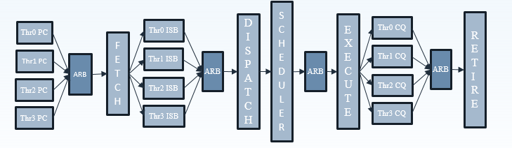
It is pretty clear that Intel's single-threaded performance remains unchallenged: the Skylake core is the widest core, keeps the most instructions in flight, and most importantly runs at the highest clockspeed. The ThunderX2 core is the one that fetches the most instructions per cycle, as it has to be able to keep 4 threads running. The fetch unit will grab 8 instructions from one thread, than grab 8 from the second thread and it will keep cycling between threads. A bad prediction could thus lower the performance of single thread significantly.


97 Comments
View All Comments
Davenreturns - Wednesday, May 23, 2018 - link
In the spec table for the AMD EPYC 7601 you have max sockets 4 and PCIe 3.0 lanes as 64. I thought the max sockets was 2 and that the total number of PCIe 3.0 lanes was 128 (64 in a dual socket machine).davegraham - Wednesday, May 23, 2018 - link
max sockets is 2 and PCIe lanes is 128 (64 from each 7601 for a combined total of 128; remember, each 7601 has 128 PCIe lanes by themselves. 64 from each are ganged together for IF in a 2P system).davegraham - Wednesday, May 23, 2018 - link
*are not *isDavenreturns - Wednesday, May 23, 2018 - link
But in a single socket motherboard system, the total PCIe lanes available from one EPYC processor is 128 which I think we are both saying is correct.Davenreturns - Wednesday, May 23, 2018 - link
The reason I think these two corrections are important and should be addressed by the author is the way the players in the market are competing. The table should read 128 PCIe lanes and 2 sockets max for EPYC. One only needs to look at AMD's EPYC One socket page to understand why it is important.https://www.amd.com/en/products/epyc-7000-series-1...
The page is filled with marketing trying to convince customers that you are actually getting a two socket server in just one socket. And yes 128 PCIe lanes are available to the customer in these one socket products as part of the reasoning.
The max number of sockets is also important. AMD and probably Cavium are both arguing that 90% of the market only needs 1 or 2 sockets. Intel doesn't agree and provides 4 or more socket configurations.
The one socket argument centers around the I/O and memory channels available in the AMD processor. Even though the table just might have typos, reviewers around the web had a hard time believing that a single chip offered 128 lanes of PCIe connectivity and I found a lot of misinformation. It continues today.
DanNeely - Wednesday, May 23, 2018 - link
AFAIK even for intel 1/2 socket machines are around 90% of their sales. They're just selling enough total server chips in total that catering to the sliver of the market that does want 4/8way configurations is still worth their time.Arnulf - Sunday, May 27, 2018 - link
Profit margins in that market segment are likely to be way higher so it's worth it for Intel as long as there is no competition, forcing prices downwards.Ryan Smith - Wednesday, May 23, 2018 - link
You are correct. Thanks for pointing that out.Davenreturns - Wednesday, May 23, 2018 - link
Thanks so much, Ryan.vanilla_gorilla - Wednesday, May 23, 2018 - link
"This is because the customers who have invested in expensive enterprise software (Oracle, SAP) are less sensitive to cost on the hardware side, so they are much less likely to change to a new hardware platform."I don't really follow the logic here. Just because you spend a lot more money on software doesn't mean you wouldn't try to save money on hardware. You don't only focus on one related expense because it's larger.