Qualcomm's New Snapdragon S4: MSM8960 & Krait Architecture Explored
by Brian Klug & Anand Lal Shimpi on October 7, 2011 12:35 PM EST- Posted in
- Smartphones
- Snapdragon
- Arm
- Qualcomm
- Krait
- MDP
- Mobile
- SoCs
Cache & Memory Hierarchy
Qualcomm has a three level exclusive cache hierarchy in Krait. The lower two levels are private per core, while the third level is shared among all cores. Qualcomm calls these caches L0, L1 and L2.
Each Krait core has an 8KB L0 cache (4KB instruction + 4KB data cache). The L0 cache is direct mapped and accessible in a single cycle. Qualcomm claims an 85% hit rate in this level 0 cache, which helps save power by not firing up the larger L1 cache. The hierarchy is exclusive so L0 data isn't necessarily duplicated in L1.
Each core also has a 32KB L1 cache (16KB instruction + 16KB data). The L1 4-way set associative and can also be accessed in a single cycle. There's no way prediction at work here. With 1 cycle latency to both L0 and L1, the primary advantage here is power.
| Krait Cache Architecture | |||||
| Size | Architecture | Frequency | |||
| L0 | 4KB + 4KB | Direct Mapped | Core | ||
| L1 | 16KB + 16KB | 4-way set associative | Core | ||
| L2 | 1MB (dual core) or 2MB (quad core) | 8-way set associative | 1.3GHz max | ||
The L2 cache is shared among all cores. In dual-core designs the L2 cache is sized at 1MB (up from 512KB in Scorpion), while quad-core Krait SoCs will have a 2MB L2. Krait's L2 cache is 8-way set associative.
While the L0 and L1 caches operate at core frequency and are on the same voltage plane as their associated core, the L2 cache is separate. To save power the L2 cache runs at its own frequency (up to 1.3GHz depending on the currently requested performance level). The L2 cache is on its own power plane and can be power gated if necessary.
Although Scorpion featured a dual-channel LPDDR2 memory controller, in a PoP configuration only one channel was available to any stacked DRAM. In order to get access to both 32-bit memory channels the OEM had to implement a DRAM on-package as well as an external DRAM on the PCB. Memory requests could be interleaved between the two DRAM, however Qualcomm seemed to prefer load balancing between the two with CPU/GPU accesses being directed to the lower latency PoP DRAM. Very few OEMs seemed to populate both channels and thus Scorpion based designs were effectively single-channel offerings.
Krait removes this limitation and now OEMs can utilize both memory channels in a PoP configuration (simply put two 32-bit DRAM die on the PoP stack) or in an external configuration. The split PoP/external DRAM organization is no longer supported. This change will hopefully mean we'll see more dual-channel Krait designs than we saw with Scorpion, which will in turn improve performance.
Process Technology and Clock Speeds
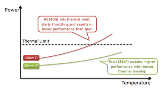
Krait will be the world's first smartphone CPU built on a 28nm process. Qualcomm is working with both TSMC and Global Foundries, although TSMC will produce the first chips. Krait will be built, at first, on TSMC's standard 28nm LP process. According to Qualcomm there's less risk associated with TSMC's non-HKMG process. Qualcomm was quick to point out that the entire MSM8960 SoC is built on a 28nm LP process compared to NVIDIA's 40nm LPG design in Kal-El. From Qualcomm's perspective, 40nm G transistors are only useful at reducing leakage at high temperatures but for the majority of the time a homogeneous LP design makes more sense.
Just like Scorpion, Krait places each core on its own voltage plane driven at its own clock frequency. Cores can be clocked independently of one another, which Qualcomm insists gives it a power advantage in many workloads.
The first implementation of Krait will be in a dual-core 1.5GHz MSM8960, however a second revision of the silicon will be introduced next year that increases clock speed to 1.7 - 2.0GHz. Qualcomm claims that at the same 1.05V core voltage, Krait can run at 1.7GHz vs. 1.55GHz for Scorpion. At these two clock speeds and at the same voltage, Qualcomm tells us that Krait consumes 265mW of power vs. 432mW running an undisclosed workload. Although it should be possible to draw more power than Scorpion under load, Krait should hopefully be able to improve overall power efficiency by completing tasks quicker and thus dropping down to idle faster than its predecessor. Smartphone and tablet battery life should remain the same at worst and improve at best, as a result.


108 Comments
View All Comments
dagamer34 - Friday, October 7, 2011 - link
Great stuff to look forward to. Some comments:1) I wasn't aware that Microsoft released DirectX 9.3. Perhaps you meant 9.0c or 9.1?
2) Why is nVidia still using a single LPDDR2 channel when everyone else has gone to dual channel memory?
I do look forward to seeing what the next generation of GPUs will provide. Seems like we've stayed in this console generation too long with cell phones having graphics nearly on par with their 200W cousins.
A5 - Friday, October 7, 2011 - link
Re: DX 9.3, you beat me to it.Ilomilo is pretty, but it's not exactly Gears or Battlefield, you know?
Ryan Smith - Friday, October 7, 2011 - link
It's actually more complex than that. When it comes to programming for Direct3D11, there are a number of different GPU feature level targets. The idea is that developers will write their application in DX11, and then have customized render backends to target each feature level they want to hit.As it stands there are 6 feature levels: 11, 10_1, 10, 9_3, 9_2, and 9_1. Unfortunately everyone has been lax in their naming standards; DirectX and Direct3D often get thrown around interchangeably, as do periods and underscores in the feature levels (since prior to D3D 11, we'd simply refer to the version of D3D). This is how you end up with DirectX 9.3 and all permutations thereof. The article has been corrected to be more technically accurate to clear this up.
In any case, 9_1 is effectively identical to Direct3D 9.0. 9_3 is somewhere between D3D 9.0b and 9.0c; it implements a bunch of extra features like multiple render targets, but the shader language is 2.x (Vertex Shader 2.0a, Pixel Shader 2.0b) rather than 3.0
partylikeits1999 - Saturday, October 8, 2011 - link
Microsoft made such a mess out of its DirectX nomenclature in the DX9 timeframe that the rest of the industry started to ignore it and invent their own. Hardly anybody even bothers to distinguish between Direct3D and DirectX anymore...they're used interchangeably, even though the former is a subset of the latter.Windows 8 requires Shader Model 3.0 to be supported by the hardware. Whether you call that 10Level9_3 or 9_3, or DX9.3, or D3D9.3, who cares...from a graphics perspective, it is all just Shader Model 3.0 in the end, whatever you want to call it. All of the Windows 8 launch chipsets from nVidia, TI and Qualcomm, including this MSM8960 will all support Shader Model 3.0 as far as I can tell.
ET - Sunday, October 9, 2011 - link
Feature level 9_3 isn't the same as Shader Model 3 support. The Qualcomm docs say DX9.3 though, which is quite confusing since it doesn't exist. That said, I agree with your assessment that it means Shader Model 3, and not feature level 9_3.felixyang - Saturday, October 8, 2011 - link
2) I believe dual channels don't give any advantage due to tegra's system bus.metafor - Friday, October 7, 2011 - link
MSM8260 and MSM8660 only have single-channel 32-bit LP-DDR2 memory, not dual.z0mb13n3d - Friday, October 7, 2011 - link
Please read:Although Scorpion featured a dual-channel LPDDR2 memory controller, in a PoP configuration only one channel was available to any stacked DRAM. In order to get access to both 32-bit memory channels the OEM had to implement a DRAM on-package as well as an external DRAM on the PCB. Memory requests could be interleaved between the two DRAM, however Qualcomm seemed to prefer load balancing between the two with CPU/GPU accesses being directed to the lower latency PoP DRAM. Very few OEMs seemed to populate both channels and thus Scorpion based designs were effectively single-channel offerings.
I can tell you with a modicum of confidence that this is true, at least partially.
Aren't you the same person who went on (ranting, obviously) about Krait using HKMG and hitting 2.5GHz next year, in another article?
ArunDemeure - Friday, October 7, 2011 - link
I suggest you stop embarassing yourself. metafor knows what he's talking about, and you clearly don't. I read that previous thread - he was pretty much spot on for everything, as you would expect. I honestly don't know why he even bothers here given the reception he's getting...Anyway unlike what the article says, the MSM8x60 indeed only has single-channel 32-bit LPDDR2. However there's a twist: Qualcomm offers it in a PoP (Package-on-Package) configuration at up to 266MHz or an 'ISM' (i.e. SiP or System-in-Package) at up to 333MHz. I wouldn't be surprised if many OEMs used the PoP for cost reasons.
I think the confusion might come from another (older) Qualcomm SoC working like the article described iirc, but this does not apply to the MSM8x60 AFAIK.
Anand Lal Shimpi - Friday, October 7, 2011 - link
Arun,This information does come from Qualcomm, although the odd PoP + external DRAM configuration (that no one seems to use) basically means that MSM8x60 is a single-channel architecture (which is why I starred it in the table above). I will ask Qualcomm once more for confirmation that this applies to MSM8x60 as well as the older single core variants.
Take care,
Anand