MIPS Technologies Updates Processor IP Lineup with Aptiv Series
by Ganesh T S on May 10, 2012 8:55 AM ESTThe interAptiv family brings multithreading to the table, something which ARM hasn't started implementing yet. As our Lava Xolo smartphone revealed, implementing simultaneous multi-threading is highly beneficial for performance, particularly in current day workloads.
MIPS claims that 3 interAptiv cores deliver performance similar to / slightly exceeding what could be obtained from 2x Cortex-A9 / 3x Cortex-A5 cores with the same silicon area. Of course, CoreMark numbers heavily favor the interAptiv cores.
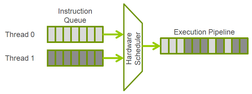
In the interAptiv family, the CPU execution pipeline is shared by multiple threads, which allows the mitigation of the performance impact of memory access latencies. Since interAptiv is targeted towards real time workloads, a hardware scheduler enables a better QoS.

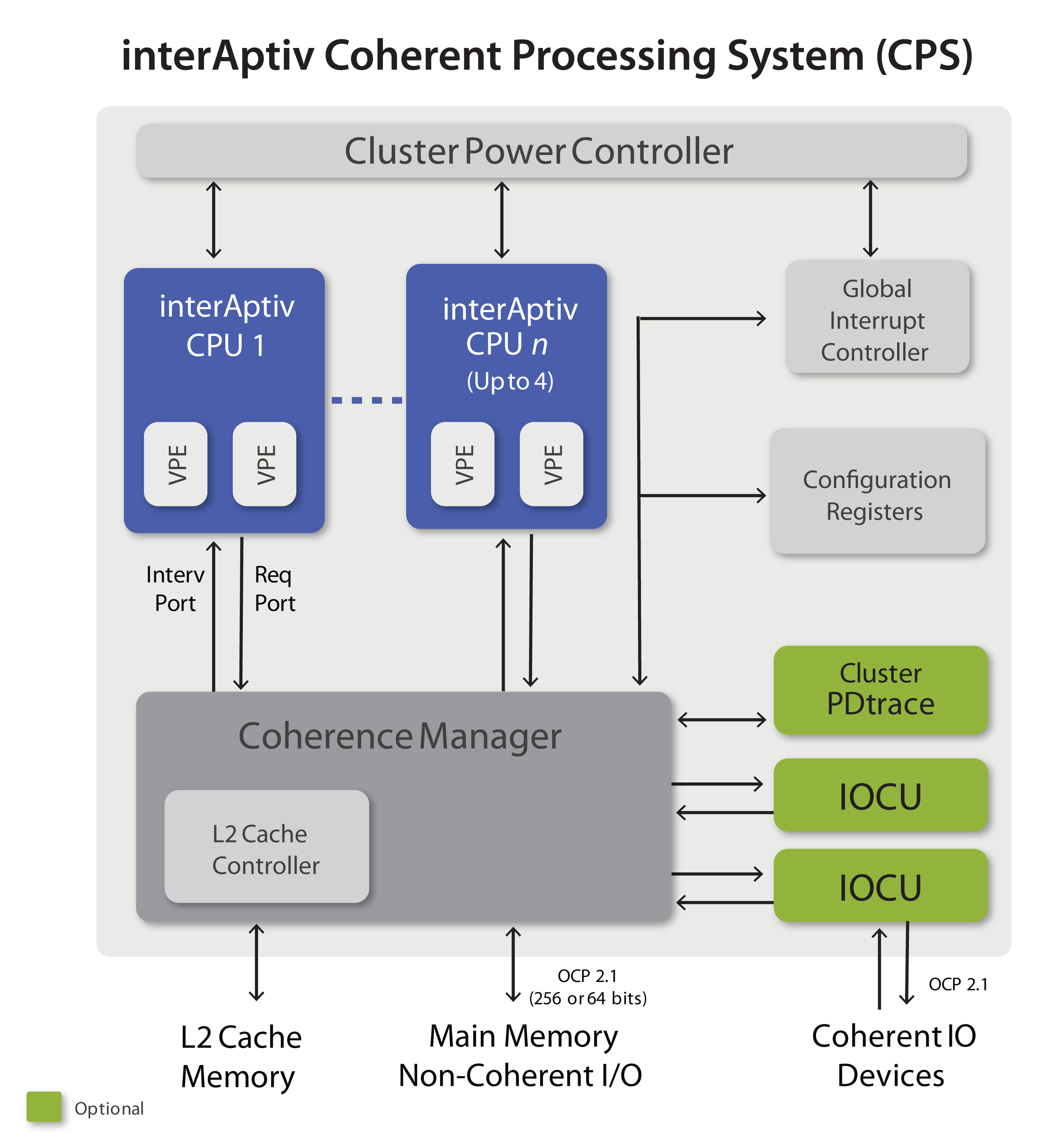
MIPS terms the threads as VPEs (virtual processing elements). The pipeline itself is 9 stages long and is in-order. An optional multi-threaded IEEE 754 FPU can be added if necessary. DSP ASE is available, as is EVA (similar to the proAptiv family). The CPS used with the multi-core interAptiv family has the same features as that used by the proAptiv.
Compared to the proAptiv, the interAptiv core architecture allows for core clock shutdown during outstanding bus requests, intelligent way selection in the L1 instruction cache and 32-bit L1 data cache access as options for power reduction. [ Update: Intelligent way selection in the L1 instruction cache is also available in the proAptiv family ]
In the TSMC 40nm G process, the interAptiv family members can run at up to 1 GHz for applications involving multi-threading with QoS and at up to 1.2 GHz for multi-threading without QoS. If DSP ASE is not desired, implementations can run at up to 1.5 GHz for networking applications. [ Update: The quoted frequency numbers are 'sweet spots' in terms of power consumption and other application specific requirements. As mentioned in the previous section, the frequency of operation can be scaled depending on customer requirements and is not related to the presence of absence of DSP ASE / QoS ]
The microAptiv architecture is a superset of the M14K/c cores with microMIPS code compression support. With integrated DSP ASE, signal processing comes in at a lower cost. There are options to implement without caches / MMUs depending on the application.

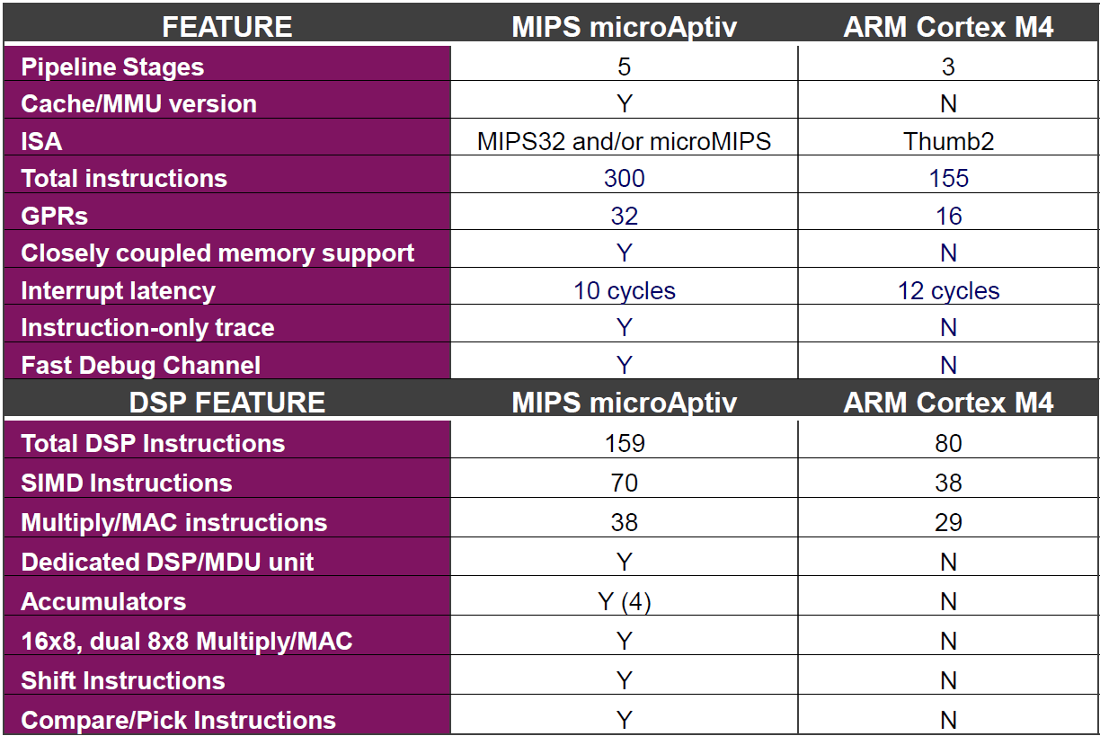
This 5 stage pipeline architecture can run at up to 400 MHz in a 65nm LP process. MIPS also presented a side-by-side comparison of the Cortex-M4 and the microAptiv family:
Obviously, the extra features don't come without an area penalty. In a 90nm LP process, Cortex-M4 has a floorplanned area of 0.17 mm2 compared to the 0.42 mm2 of the microAptiv MCU (cacheless version). [ Update: MIPS claims that the area numbers are not apples-to-apples comparison. Under similar implementation conditions in 90LP - read, area optimized - MIPS expects the microAptiv family to have only 0.01 mm2 extra area. Our data is from ARM's Cortex-M4 specifications. We agree it is difficult to compare the area requirements, but readers should note that there is no free lunch when it comes to feature set vs. die area ]


40 Comments
View All Comments
sicofante - Thursday, May 10, 2012 - link
What's the meaning of IP here? Thanks.Homeles - Thursday, May 10, 2012 - link
Intellectual Property.http://en.wikipedia.org/wiki/Semiconductor_intelle...
SydneyBlue120d - Thursday, May 10, 2012 - link
Is there something like Mali, PowerVR and so on? And what about Cell modems (LTE and so on)? Thanks.Arnulf - Thursday, May 10, 2012 - link
This is precisely why AMD should be the buyer of MIPS. They can contribute their (ATI's) GPU expertise and AMD's with hybrid processing ... this would be a killer combination.quadrivial - Thursday, May 10, 2012 - link
I agree that AMD and MIPS could be a great combination. I don't know if they could outbid China.The Chinese scientists who started the first (or at least the first to make tech news headlines over here) major Chinese-designed processor had the pick of any architecture they wanted (they weren't paying licensing fees anyway) and they still chose MIPS for the Loongson processors (which are now in devices ranging from small consumer devices to a petaflop supercomputer).
Penti - Thursday, May 10, 2012 - link
AMD/ATi already sold their mobile GPU business to Qualcomm and Broadcom respectably and has none left. They couldn't contribute a great deal here. As they already did to the field. These chips and MIPS Tech itself doesn't compete for the mobile space and any third party building such solutions will use basebands with ARM-cores and normal third party Silicon-IP GPUs. AMD also got rid of their MIPS-based network processors a good while ago. Those building MIPS network processors also do their own architectures (designs) and only license the ISA/Patents. They do things like 16-core 64-bit MIPS processors. Sigma Designs is one company that uses MIPS IP-cores with PowerVR graphics. Some also use Vivante IP/synthesizable GPUs. No different to ARM here except maybe less choice in the market and that it is up to Qualcomm or Broadcom to ship cores with Adreno or Broadcom Videocore/Xilleon. They won't be delivered as IP cores.Also while Broadcom and Qualcomm greatly build on and enhanced their custom design (gpus) from AMD designs that where not exactly Radeon based but other custom designs to develop them into to highly developed and fast gpus, for example nVidia didn't really do that by building "geforce-based" gpus on Tegra where it is greatly under powered and the wrong design for mobiles pretty much. AMD gpus would be disastrous to scale down too. Plus they can sell x86/x64 CPUs / APUs with AMD GPUs for the Android tablet market or Tablet PC market already. They have no reason to go ARM or MIPS (again) just as Intel has no reason to go back to ARM (XScale). They might for servers, but not clients. They can deliver other solutions based on their existing tech there.
Guspaz - Friday, May 11, 2012 - link
MIPS doesn't make the SoC, just the CPU. There's nothing stopping anybody from putting a PowerVR GPU into an SoC with a MIPS CPU.Think about it this way: ARM makes the Cortex A9, but they don't make any chips. nVidia makes the Tegra, TI makes the OMAP, Samsung makes the Exynos, Apple makes the A series, etc. The same thing is true here with MIPS. They just give you a set of blueprints for a CPU and you make it yourself.
sheh - Thursday, May 10, 2012 - link
I had the impression all those routers were running ARM. What's that about no multithreading on ARM? In terms of something like Intel's Hyperthreading?BTW, "upto" -> "up to".
Arnulf - Thursday, May 10, 2012 - link
Most use MIPS chips (something along the lines of an R4000 relative).Jaybus - Thursday, May 10, 2012 - link
Yes, I believe so. ARM has only test-and-set, etc primitive instructions for atomic operations, meaning the OS is essentially performing all aspects of multithreading and context switches are expensive. Unlike x86, it has no hardware allowing for fast context switching.