The Snapdragon 855 Performance Preview: Setting the Stage for Flagship Android 2019
by Andrei Frumusanu on January 15, 2019 8:00 AM EST- Posted in
- Mobile
- Qualcomm
- Smartphones
- SoCs
- 7nm
- Snapdragon 855

As we get ever closer to the releases of various Android vendor’s newest generation devices, Qualcomm continues its tradition of showcasing the performance of its newest generation SoC ahead of time, giving us a preview and a glimpse of what to expect of the upcoming commercial devices. This year, the company has shuffled the schedule around a bit, and instead of hosting the event at their San Diego headquarters, and we were able to get a hands-on with the Snapdragon 855 at CES before the show had started. Today we’re be looking in quite extensive detail on how exactly the new Snapdragon chipset performs, as well as shedding some light on some important unanswered technical questions on some aspects of the SoC.
It’s been roughly a little over a month now since Qualcomm officially announced the Snapdragon 855 in Hawaii, and we had posted extensive coverage on the event and the various announcements that took place:
Full Coverage
Day One
- Qualcomm Tech Summit, Day 1 Live Blog (Starts at 2pm ET)
- Qualcomm Tech Summit, Day 1: Announcing 5G Partnerships and Snapdragon 855
- The Verizon and AT&T 5G Setups at Qualcomm’s Snapdragon Summit
- 5G Mobile Hotspots: Netgear for AT&T and inseego for Verizon
- A Quick Look at Qualcomm’s 5G Smartphone Reference Design
- Implementing 5G in the UK: EE Trial Sites and First Cities
- Samsung’s 5G Smartphone Prototype: Don’t Mention The Notch
- Moto 5G Mod at Snapdragon Summit: Lots of Antennas, and S855 Inside?
Day Two
- Qualcomm Tech Summit, Day 2 Live Blog (Starts at 2pm ET)
- Qualcomm Tech Summit, Day 2: Snapdragon 855 Mobile Platform
- The Qualcomm Snapdragon 855 Pre-Dive: Going Into Detail on 2019's Flagship Android SoC
- OnePlus: Dual Product Lines, Cost of 5G, and Translation Errors
- Snapdragon 855 Power Consumption Demo, But
- Snapdragon 855: 802.11ax-Ready / Wi-Fi 6 Demonstrations
Day Three
- Qualcomm Tech Summit, Day 3 Live Blog (Starts at 2pm ET)
- Spotted: Qualcomm Snapdragon 8cx Wafer on 7nm
- Qualcomm Tech Summit, Day 3: Snapdragon 8cx, the New ACPC SoC
For anyone who might have missed it, if there’s any one specific article that I would recommend reading before heading in directly to the results of the benchmarking session, then it’s our in-depth piece summarising the disclosed specifications of the new Snapdragon 855.
SoC Overview & CPU Recap
| Qualcomm Snapdragon Flagship SoCs 2018-2019 | |||
| SoC |
Snapdragon 855 |
Snapdragon 845 | |
| CPU | 1x Kryo 485 Gold (A76 derivative) @ 2.84GHz 1x512KB pL2 3x Kryo 485 Gold (A76 derivative) @ 2.42GHz 3x256KB pL2 4x Kryo 485 Silver (A55 derivative) @ 1.80GHz 4x128KB pL2 2MB sL3 |
4x Kryo 385 Gold (A75 derivative) @ 2.8GHz 4x256KB pL2 4x Kryo 385 Silver (A55 derivative) @ 1.80GHz 4x128KB pL2 2MB sL3 |
|
| GPU | Adreno 640 @ ?MHz | Adreno 630 @ 710MHz | |
| Memory | 4x 16-bit CH @ 2133MHz LPDDR4x 34.1GB/s 3MB system level cache |
4x 16-bit CH @ 1866MHz LPDDR4x 29.9GB/s 3MB system level cache |
|
| ISP/Camera | Dual 14-bit Spectra 380 ISP 1x 48MP or 2x 22MP |
Dual 14-bit Spectra 280 ISP 1x 32MP or 2x 16MP |
|
| Encode/ Decode |
2160p60 10-bit H.265 HDR10, HDR10+, HLG 720p480 |
2160p60 10-bit H.265 720p480 |
|
| Integrated Modem | Snapdragon X24 LTE (Category 20) DL = 2000Mbps 7x20MHz CA, 256-QAM, 4x4 UL = 316Mbps 3x20MHz CA, 256-QAM |
Snapdragon X20 LTE (Category 18/13) DL = 1200Mbps 5x20MHz CA, 256-QAM, 4x4 UL = 150Mbps 2x20MHz CA, 64-QAM |
|
| Mfc. Process | 7nm (N7) | 10nm LPP | |
Summarising the Snapdragon 855 quickly, at the heart of the new 7nm chipset we find four new Kryo 485 CPUs based on Arm’s new Cortex A76 cores. The new CPU cores are derivatives of the designs Arm makes available by default: Here Qualcomm takes advantage of the “Built on Arm Cortex Technology” license which allows vendors to demand changes to the IP based on a set of microarchitectural tuneables that Arm makes available. Even though the Snapdragon 855’s Kryo 485 is the third generation of such a derivative core from Qualcomm, it represents the first instance of the company actually talking about what kind of microarchitectural changes have been made to the CPUs. The Kryo 485 Cortex A76 derivatives increase the re-order buffer from Arm’s default 128 entries to a higher, undisclosed figure. Qualcomm has also revealed that the prefetchers have been optimised for better efficiency, although again we don’t have any details on how exactly this has been achieved. Finally, as I’ve understood it, the branch data structures have also seen an improvement over the default A76 configuration.

Although the SoC still comes in a “4+4” big.LITTLE high-level core configuration, the big cores in the S855 aren’t actually all equal: Here Qualcomm has gone for a rather exotic 1+3+4 configuration, in which one of the big cores is implemented with a higher frequency physical design reaching 2857MHz, all while also employing a larger L2 cache of 512KB. The remaining three big cores max out at 2439MHz and are only equipped with 256KB L2 caches. Qualcomm does clock this 1+3 configuration differently with asynchronous clock planes, however the cores still share the same voltage plane. Here the company explains that this is a compromise between power efficiency benefits, and cost of implementation complexity as well as supporting power delivery components (Adding an extra voltage plane adds another PMIC rail with inductors & capacitors).
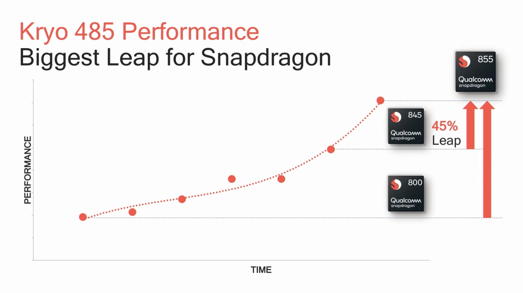
The Kryo 485 in the S855 promises to be Qualcomm’s biggest performance jump ever, advertising a 45% jump in performance compared to the Snapdragon 845. As we had discussed it in our launch article, this figure seems to coincide with the performance jump the Kirin 980 saw over the Snapdragon 845, which makes sense given that the two new SoCs both employ the newest generation A76 CPU at similar clocks.
The Snapdragon 855 QRD

Today’s testing platform is Qualcomm’s new Snapdragon 855 QRD (Qualcomm Reference Design). This year’s QRD design is probably Qualcomm’s most “commercial-device-like” ever as other than the more robustly built bezels, you would have a hard time noticing that this a reference platform – at least on the hardware side. The company stated that the QRD as tested should be a near representation of what to expect of commercial device – but of course vendors might still diverge from this as they may change the underlying software.
We’ve had a limited hands-on time with the devices, and although we managed to do a lot with them, some of the more time-intensive testing such as GPU sustained performance testing were out of the scope of today’s session.
The Big Question For The Snapdragon 855 : Memory Latency
One of the more odd developments that Qualcomm introduced with the Snapdragon 845 last year was the addition of a new 3MB system level cache that sits in front of the memory controllers as a new cache hierarchy. This new block is meant to serve as a SoC-wide buffer for the various IP blocks, reducing the amount of expensive DRAM memory accesses and thus improving power efficiency of the system. As well as improving power efficiency, it could in theory also serve as a booster for performance. The most famous use of such a system cache is Apple’s own A-series chips where we’ve seen this kind of IP block used ever since the A7.
Qualcomm’s introduction of such an IP block in the Snapdragon 845 was exciting to see, however this came as a double-edged sword as it had also introduced a 30% regression (In comparison to the Snapdragon 835) in DRAM memory latency, which may have limited some of the performance aspects of the A75-based CPU last year.
The new Snapdragon 855 unfortunately doesn’t seem to have made any major improvements in this regard as Qualcomm had confirmed that the IP block is the same as the one used in the Snapdragon 845.
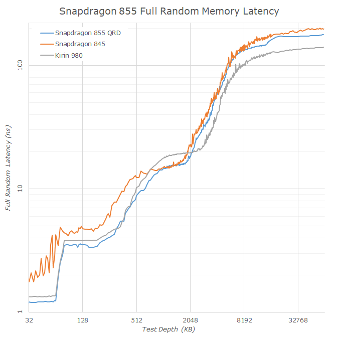
To investigate the differences between the Snapdragon 845, 855 and also the Kirin 980, we make use of latency test. First off, let’s view the memory hierarchy in a logarithmic latency graph, better visualising the various latency jumps between hierarchies:
Between the Snapdragon 845 and the new 855, we now see the increased L2 cache of the Kryo 485 Prime core at 512KB, an increase over the 256KB size on the previous generation performance core. What is also visible is that the L2 latency has improved, even though both chipsets are clocked near to each other at ~2.8GHz.
The DSU L3 cache on both the Snapdragon 845 and 855 are identical at 2MB in size: Again what’s interesting here to see is that the latency on this part of the cache hierarchy seems to be identical between both SoCs. This is in contrast to the 4MB L3 of the Kirin 980 which, albeit bigger, seems to be 20% slower.
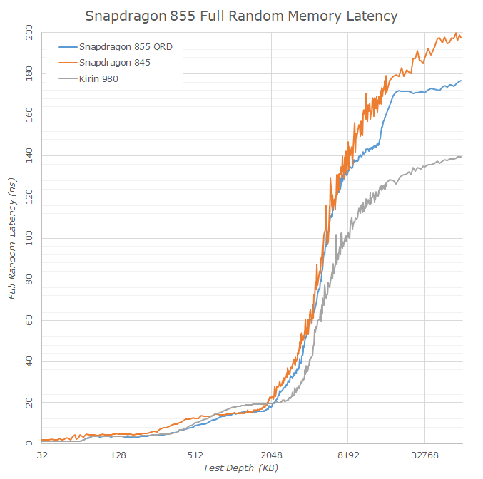
Moving onto the linear graph, here we can see the difference in DRAM latency in a clearer fashion. The Snapdragon 855 does seem to slightly improve memory latency over the 845, however this might just be an effect of the newer 2133MHz LPDDR4X memory that represents a 14% speed boost over the 1866MHz memory of last year’s devices.
Critically though, is the comparison to the Kirin 980 which employs the same CPU microarchitecture, and the same 2133MHz memory as the Snapdragon 855. Here Qualcomm still shows a notable latency regression in memory latency over the competition, whose effects will be interesting to analyse in the following pages.


132 Comments
View All Comments
genekellyjr - Wednesday, January 16, 2019 - link
You might be clueless too! There weren't any "4k rendering" benchmarks in that link - but there were 4k encoding benchmarks.And as for that encoding performance you are apparently referencing, it is definitely using fixed function encoders - it's not the CPU performance as Geekbench tests use (and I want to stress cross-platform Geekbench isn't 1:1 scoring - you'll never find Andandtech comparing various CPU architectures with Geekbench as it even uses fixed function resources like AES in its crypto stuff). And the speeds the laptops show definitely point to a CPU encoder being used. A fixed function encoder will barely hit the CPU, while CPU encoding will max those cores at 100%. The CPU encoding is higher quality at the cost of heat and speed.
Recently Adobe updated Premier to support Intel's fixed function encoder (called quick sync) read here http://www.dvxuser.com/V6/showthread.php?362263-Ad... post #8 - and Rush may not have gotten that update yet or the benchmark site referenced didn't update their program https://www.laptopmag.com/reviews/laptops/new-ipad... but I managed to find a benchmark for the quick sync in Premier https://forums.creativecow.net/thread/335/101459 - and Intel's quick sync fixed function stuff is all relatively the same afaik so the desktop CPU has less of an impact - gives a 1:20 min 4K -> 1080p conversion at 91 sec w/ CPU and 45 sec w/ fixed function, scale that up to 12 min (x9) and we get 13:39 w/ CPU (it's a nice CPU, i7-8700K) and the fixed function encoder gets 6:45. It'll probably scale pretty linearly. So 6:45 vs 7:47 with fixed function encoding - which isn't comparing CPUs at all at this point but rather their fixed function encoder!
So the iPad has some nice hardware, sure, but it's not outperforming Intel's brand new MB Pro 13" by leaps and bounds. They'll probably be about the same speed with fixed function encoding and the MB Pro 13" will win in a non-encoder setting thanks to its increased TDP.
darkich - Friday, January 18, 2019 - link
Okay.. So in short, the A12X is "about the same" in CPU performance as Intel's actively cooled, CPU-specific and twice more power hungry chip while also having a 1+TFLOPS GPU, 4G modem and advanced ISP on the same die.Overall, if that is what you call "nice", then Intel's hardware is what?
Trash.
Rudde - Friday, January 18, 2019 - link
Let's compare Intel i7-8500Y and Apple A12X. The i7-8500Y is a dual core 5W 14nm notebook/tablet processor. A12X is a octa core 7nm tablet processor with unknown power usage. 8500Y uses the x86-64 instruction set, while A12X uses ARMv8. They have very few benchmarks in common, which introduces notable amounts of uncertainty.Let's start with Geekbench 4.1/4.2 Single threaded:
8500Y scored 4885 and A12X 4993. A12X leads with 2%, which is within margin of error.
Same benchmark, but multithreaded:
8500Y scored 8225 and A12X 17866. A12X demolishes the dual core with 117% higher performance. This is clearly because of the 4-core-cluster in A12X having double core count compared with the dual core 8500Y.
Next up we have Mozilla Kraken 1.1 showing browser performance:
8500Y scores 1822ms and A12X 609ms. The A12X took 67% less time to complete the task, which amounts to a 199% increase in performance.
Octane V2 is another browser performance benchmark:
8500Y scores 24567 and A12X 45080. A12X bests the Intel cpu by 83%.
3D Mark has two versions of Ice Storm Physics and unfortunately our processors use different versions. They use the same resolution however.
8500Y scores 25064 in standard physics and A12X 39393 in unlimited physics. A12X scores a 57% lead.
It's hard to establish system performance with such a limited amount of benchmarks. Geekbench and 3DMark are synthetics and the two others show browser performance.
The processors are equal in ST, but the A12Xs higher core count allows it to double the 8500Ys MT score. The A12X outpaces the 8500Y in 3dMark. The A12X is clearly superior in browser performance. Apples A12 drops closer to the Intel in synthetics, but performs similar to it's larger sibling in web benchmarks.
Winner: A12X
Nemaca - Tuesday, January 15, 2019 - link
Overall, the 855 was thought to be head and shoulders above Kirin, but it seems that it will be on the same level at best.I'm typing this from my already heavily used mate 20pro, so if the US wouldn't nuke Huawei global-wide right now, the Kirin would certainly push ahead, which I hope it will do, since it seems more competitive price-wise.
Huawei bypassed the power issue with larger batteries, but to be honest, the Kirin doesn't seem to be that hungry anyway.
For me, the 855 is a letdown, I was hoping for more, but it seems my mate20pro will be relevant for longer then I thought, so not too bad of a news, I guess.
Thank you, Andrei, for the in-depth review!
Achtung_BG - Wednesday, January 16, 2019 - link
Snapdragon 855 .......https://youtu.be/mqFLXayD6e8
darkich - Tuesday, January 15, 2019 - link
This here proves once and for all that your system performance benchmarks are just bogus and irrelevant.Are we seriously supposed to believe that Snapdragon actually made a lower performing chipset than their previous one?
BS
darkich - Tuesday, January 15, 2019 - link
*Qualcomm, not SnapdragonIcehawk - Tuesday, January 15, 2019 - link
It's happened before in the chase for efficiencynpp - Tuesday, January 15, 2019 - link
I really doubt we’ll see battery life improve much with this generation. Hint - 5G. Maybe that’s why 855 focuses on overall efficiency, and the GPU gains are modest. Let’s hope I’m wrong.Impulses - Tuesday, January 15, 2019 - link
Yeah, that's the big wrench in the works... Hopefully there's at least *some* flagships without 5G! Though I doubt I'll be looking for an upgrade from my Pixel 3 this year or next.