The Intel 12th Gen Core i9-12900K Review: Hybrid Performance Brings Hybrid Complexity
by Dr. Ian Cutress & Andrei Frumusanu on November 4, 2021 9:00 AM ESTIntel Disabled AVX-512, but Not Really
One of the more interesting disclosures about Alder Lake earlier this year is that the processor would not have Intel’s latest 512-bit vector extensions, AVX-512, despite the company making a big song and dance about how it was working with software developers to optimize for it, why it was in their laptop chips, and how no transistor should be left behind. One of the issues was that the processor, inside the silicon, actually did have the AVX-512 unit there. We were told as part of the extra Architecture Day Q&A that it would be fused off, and the plan was for all Alder Lake CPUs to have it fused off.
Part of the issue of AVX-512 support on Alder Lake was that only the P-cores have the feature in the design, and the E-cores do not. One of the downsides of most operating system design is that when a new program starts, there’s no way to accurately determine which core it will be placed on, or if the code will take a path that includes AVX-512. So if, naively, AVX-512 code was run on a processor that did not understand it, like an E-core, it would cause a critical error, which could cause the system to crash. Experts in the area have pointed out that technically the chip could be designed to catch the error and hand off the thread to the right core, but Intel hasn’t done this here as it adds complexity. By disabling AVX-512 in Alder Lake, it means that both the P-cores and the E-cores have a unified common instruction set, and they can both run all software supported on either.
There was a thought that if Intel were to release a version of Alder Lake with P-cores only, or if a system had all the E-cores disabled, there might be an option to have AVX-512. Intel shot down that concept almost immediately, saying very succinctly that no Alder Lake CPU would support AVX-512.
Nonetheless, we test to see if it is actually fused off.
On my first system, the MSI motherboard, I could easily disable the E-cores. That was no problem, just adjust the BIOS to zero E-cores. However this wasn’t sufficient, as AVX-512 was still clearly not detected.
On a second system, an ASUS motherboard, there was some funny option in the BIOS.
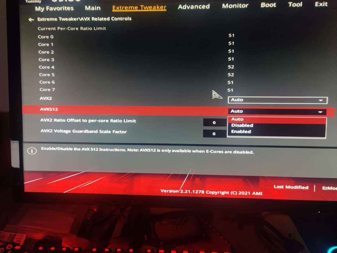
Well I’ll be a monkey’s uncle. There’s an option, right there, front and centre for AVX-512. So we disable the E-cores and enable this option. We have AVX-512 support.
For those that have some insight into AVX-512 might be aware that there are a couple of dozen different versions/add-ons of AVX-512. We confirmed that the P-cores in Alder Lake have:
- AVX512-F / F_X64
- AVX512-DQ / DQ_X64
- AVX512-CD
- AVX512-BW / BW_X64
- AVX512-VL / VLBW / VLDQ / VL_IFMA / VL_VBMI / VL_VNNI
- AVX512_VNNI
- AVX512_VBMI / VBMI2
- AVX512_IFMA
- AVX512_BITALG
- AVX512_VAES
- AVX512_VPCLMULQDQ
- AVX512_GFNI
- AVX512_BF16
- AVX512_VP2INTERSECT
- AVX512_FP16
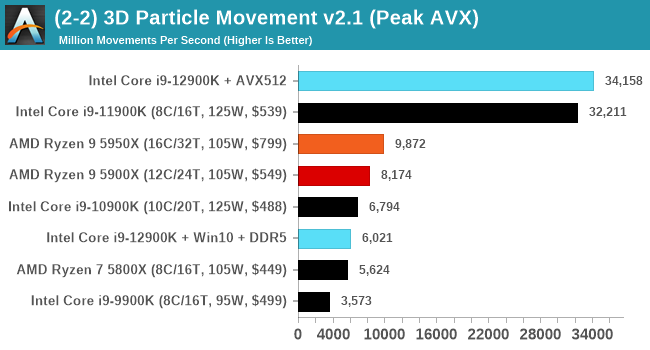
This is, essentially, the full Sapphire Rapids AVX-512 support. That makes sense, given that this is the same core that’s meant to be in Sapphire Rapids (albeit with cache changes). The core also supports dual AVX-512 ports, as we’re detecting a throughput of 2 per cycle on 512-bit add/subtracts.
For performance, I’m using our trusty 3DPMAVX benchmark here, and compared to the previous generation Rocket Lake (which did have AVX-512), the score increases by a few percent in a scenario which isn’t DRAM limited.
Now back in that Rocket Lake review, we noted that the highest power consumption observed for the chip was during AVX-512 operation. At that time, our testing showcased a big +50W jump between AVX2 and AVX-512 workloads. This time around however, Intel has managed to adjust the power requirements for AVX-512, and in our testing they were very reasonable:
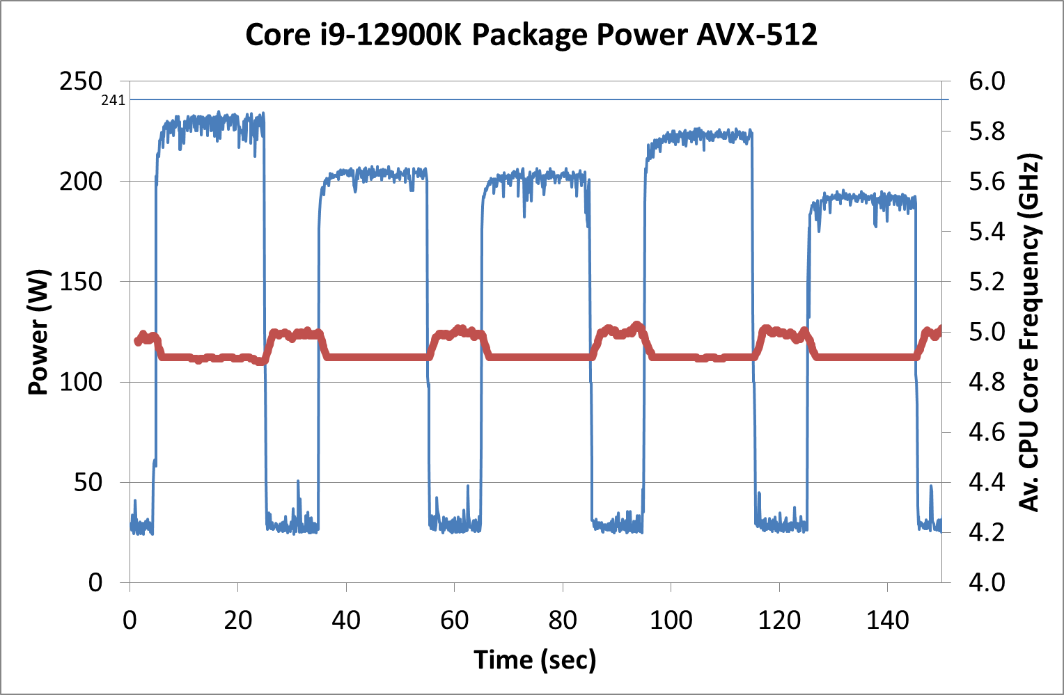
In this graph, we’re showing each of the 3DPM algorithms running for 20 seconds, then idling for 10 seconds. Each one has a different intensity of AVX-512, hence why the power is up and down. IN each instance, the CPU used an all-core turbo frequency of 4.9 GHz, in line with non-AVX code, and our peak power observed is actually 233 W, well below the 241 W rated for processor turbo.
Why?
So the question then refocuses back on Intel. Why was AVX-512 support for Alder Lake dropped, and why were we told that it is fused off, when clearly it isn’t?
Based on a variety of conversations with individuals I won’t name, it appears that the plan to have AVX-512 in Alder Lake was there from the beginning. It was working on early silicon, even as far as ES1/ES2 silicon, and was enabled in the firmware. Then for whatever reason, someone decided to remove that support from Intel’s Plan of Record (POR, the features list of the product).
By removing it from the POR, this means that the feature did not have to be validated for retail, which partly speeds up the binning and testing/validation process. As far as I understand it, the engineers working on the feature were livid. While all their hard work would be put to use on Sapphire Rapids, it still meant that Alder Lake would drop the feature and those that wanted to prepare for Alder Lake would have to remain on simulated support. Not only that, as we’ve seen since Architecture Day, it’s been a bit of a marketing headache. Whoever initiated that dropped support clearly didn’t think of how that messaging was going to down, or how they were going to spin it into a positive. For the record, removing support isn’t a positive, especially given how much hullaballoo it seems to have caused.
We’ve done some extensive research on what Intel has done in order to ‘disable’ AVX-512. It looks like that in the base firmware that Intel creates, there is an option to enable/disable the unit, as there probably is for a lot of other features. Intel then hands this base firmware to the vendors and they adjust it how they wish. As far as we understand, when the decision to drop AVX-512 from the POR was made, the option to enable/disable AVX-512 was obfuscated in the base firmware. The idea is that the motherboard vendors wouldn’t be able to change the option unless they specifically knew how to – the standard hook to change that option was gone.
However, some motherboard vendors have figured it out. In our discoveries, we have learned that this works on ASUS, GIGABYTE, and ASRock motherboards, however MSI motherboards do not have this option. It’s worth noting that all the motherboard vendors likely designed all of their boards on the premise that AVX-512 and its high current draw needs would be there, so when Intel cut it, it meant perhaps that some boards were over-engineered with a higher cost than needed. I bet a few weren’t happy.
Update: MSI reached out to me and have said they will have this feature in BIOS versions 1.11 and above. Some boards already have the BIOS available, the rest will follow shortly.
But AVX-512 is enabled, and we are now in a state of limbo on this. Clearly the unit isn’t fused off, it’s just been hidden. Some engineers are annoyed, but other smart engineers at the motherboard vendors figured it out. So what does Intel do from here?
First, Intel could put the hammer down and execute a scorched earth policy. Completely strip out the firmware for AVX-512, and dictate that future BIOS/UEFI releases on all motherboards going forward cannot have this option, lest the motherboard manufacturer face some sort of wrath / decrease in marketing discretionary funds / support. Any future CPUs coming out of the factory would actually have the unit fused out, rather than simply turned off.
Second, Intel could lift the lid, acknowledge that someone made an error, and state that they’re prepared to properly support it in future consumer chips with proper validation when in a P-core only mode. This includes the upcoming P-core only chips next year.
Third, treat it like overclocking. It is what it is, your mileage may vary, no guarantee of performance consistency, and any errata generated will not be fixed in future revisions.
As I’ve mentioned, apparently this decision didn’t go down to well. I’m still trying to find the name of the person/people who made this decision, and get their side of the story as to technically why this decision was made. We were told that ‘No Transistor Left Behind’, except these ones in that person’s mind, clearly.


474 Comments
View All Comments
Wrs - Friday, November 5, 2021 - link
Not sure if you know what TCO is. It includes electricity and some $ allotment for software support of the hardware. Most end users don't directly deal with the latter (how many $ is a compatibility headache?) and don't own a watt-meter to calculate the former.That said, what's wrong with reusing DDR4, adapting an AM4 cooler with an LGA 1700 bracket, and reusing the typically oversized PSU? AT shows DDR4 lagging, but most DDR4 out there is way faster than 3200 CL20. That's why other review sites say DDR4 wins most benches. No reasonable user buys a 12900k or 12600k to pair with JEDEC RAM timings!
Really the only cost differentiator is the CPU + mobo. ADL and Zen3 are on very similar process nodes. One is not markedly more efficient than the other unless the throttle is pushed very differently, or in edge cases where their architectural differences matter.
isthisavailable - Friday, November 5, 2021 - link
Wake me up when intel stop K series nonsense and their motherboards stop costing twice as much as AMD only to be useless when next gen chips arrive.mode_13h - Friday, November 5, 2021 - link
Intel always gives you 2 CPU generations on any new socket. The only exception to that we've seen was Haswell, due to their cancellation of desktop Broadwell.mode_13h - Friday, November 5, 2021 - link
And besides, they had to change the socket for PCIe 5.0 and DDR5, if not also other reasons.This wasn't like the "fake" change between Kaby Lake and Coffee Lake (IIRC, some industrial mobo maker actually produced a board that could support CPUs all the way from Skylake to Coffee Lake R).
Oxford Guy - Friday, November 5, 2021 - link
So...Are we no longer going to see all the benchmark hype over AVX-512 in consumer CPU reviews?
mode_13h - Friday, November 5, 2021 - link
I think we will. They devoted a whole page to it, and benchmarked it anyway.And Ian's 3DPM benchmark is still a black box. No one knows precisely what it measures, or that it casts AVX2 performance in a fair light. I will call for him to opensource it, for as long as he continues using it.
alpha754293 - Friday, November 5, 2021 - link
Note for the editorial team:On the page titled: "Power: P-Core vs E-Core, Win10 vs Win11" (4th page), the last graph on the page has AMD Ryzen 9 5900X twice.
The second 5900X I think is supposed to be the 5950X.
Just letting you know.
Thanks.
GeoffreyA - Friday, November 5, 2021 - link
For those proclaiming the funeral of AMD, remember, this is like a board game. Intel is now ahead. When AMD moves, they'll be ahead. Ad infinitum.As for Intel, well done. Golden Cove is solid, and I'm glad to see a return to form. I expected Alder Lake to be a disaster, but this was well executed. Glad, too, it's beating AMD. For the sake of pricing and IPC, we need the two to give each other a good hiding, alternately. Next, may Zen 3+ and 4 send Alder and Raptor back to the dinosaur age! And may Intel then thrash Zen 4 with whatever they're baking in their labs! Perhaps this is the sort of tick-tock we need.
mode_13h - Friday, November 5, 2021 - link
> Intel is now ahead.Let's see how it performs within the same power envelope as AMD. That'll tell us if they're truly ahead, or if they're still dependent on burning more Watts for their performance lead.
GeoffreyA - Saturday, November 6, 2021 - link
Oh yes. Under the true metric of performance per watt, AMD is well ahead, Alder Lake taking something to the effect of 60-95% more power to achieve 10-20% more performance than Ryzen. And under that light, one would argue it's not a success. Still, seeing all those blue bars, I give it the credit and feel it won the day.Unfortunately for Intel and fans, this is not the end of AMD. Indeed, Lisa Su and her team should celebrate: Golden Cove shows just how efficient Zen is. A CPU with 4-wide decode and 256-entry ROB, among other things, is on the heels of one with 6-wide decode and a 512-entry ROB. That ought to be troubling to Pat and the team. Really, the only way I think they can remedy this is by designing a new core from scratch or scaling Gracemont to target Zen 4 or 5.